SLES032E June 2002 – September 2014 THS8200
PRODUCTION DATA.
- 1 Device Overview
- 2 Revision History
- 3 Terminal Configuration and Functions
-
4 Specifications
- 4.1 Absolute Maximum Ratings
- 4.2 Handling Ratings
- 4.3 Recommended Operating Conditions
- 4.4 Power Consumption Summary
- 4.5 Power Supply
- 4.6 Digital Inputs, DC Characteristics
- 4.7 Analog (DAC) Outputs
- 4.8 Nonlinearity
- 4.9 Analog Output Bandwidth (sinx/x corrected) at fS = 205 MSPS
- 4.10 Output Compliance vs Full-Scale Adjustment Resistor Value
- 4.11 Vertical Sync of the HDTV 1080I Format Preset in First and Second Field, and Horizontal Line Waveform Detail
-
5 Functional Overview
- 5.1
Data Manager (DMAN)
- 5.1.1 Interpolating Finite Impulse Responses Filter (IFIR)
- 5.1.2 Color-Space Conversion (CSC)
- 5.1.3 Clip/Shift/Multiplier (CSM)
- 5.1.4 Digital Multiplexer (DIGMUX)
- 5.1.5 Display Timing Generator (DTG)
- 5.1.6 Clock Generator (CGEN)
- 5.1.7 Clock Driver (CDRV)
- 5.1.8 I2C Host Interface (I2CSLAVE)
- 5.1.9 Test Block (TST)
- 5.1.10 D/A Converters (DACs)
- 5.1
Data Manager (DMAN)
-
6 Detailed Functional Description
- 6.1 Data Manager (DMAN)
- 6.2 Input Interface Formats
- 6.3 Clock Generator (CGEN)/Clock Driver (CDRV)
- 6.4 Color Space Conversion (CSC)
- 6.5 Clip/Shift/Multiplier (CSM)
- 6.6 Interpolating Finite Impulse Response Filter (IFIR)
- 6.7
Display Timing Generator (DTG)
- 6.7.1 Overview of Functionality
- 6.7.2 Functional Description
- 6.7.3
DTG Line Type Overview
- 6.7.3.1 HDTV Mode
- 6.7.3.2 Active Video
- 6.7.3.3 FULL NTSP (Full Normal Tri-Level Sync Pulse)
- 6.7.3.4 NTSP NTSP (Normal Tri-Level Sync Pulse/Normal Tri-Level Sync Pulse)
- 6.7.3.5 BTSP BTSP (Broad Pulse and Tri-Level Sync Pulse/Broad Pulse and Tri-Level Sync Pulse)
- 6.7.3.6 NTSP BTSP (Normal Tri-Level Sync Pulse/ Broad Pulse and Tri-Level Sync Pulse)
- 6.7.3.7 BTSP NTSP (Broad Pulse and Tri-Level Sync Pulse/Normal Tri-Level Sync Pulse)
- 6.7.3.8 Full BTSP (Full Broad Pulse and Tri-Level Sync Pulse)
- 6.7.3.9 SDTV Mode
- 6.7.3.10 NEQ_NEQ (Negative Equalization Pulse/Negative Equalization Pulse)
- 6.7.3.11 FULL_BSP (Full Broad Sync Pulse)
- 6.7.3.12 BSP_BSP (Broad Sync Pulse/Broad Sync Pulse)
- 6.7.3.13 FULL_NSP (Full Normal Sync Pulse)
- 6.7.3.14 NEQ_BSP (Negative Equalization Pulse/Broad Sync Pulse)
- 6.7.3.15 BSP_NEQ (Broad Sync Pulse/Negative Equalization Pulse)
- 6.7.3.16 FULL_NEQ (Full Negative Equalization Pulse)
- 6.7.3.17 NSP_ACTIVE (Normal Sync Pulse/Active Video)
- 6.7.3.18 ACTIVE_NEQ (Active Video/Negative Equalization Pulse)
- 6.7.3.19 ACTIVE VIDEO
- 6.8
D/A Conversion
- 6.8.1 RGB Output Without Sync Signal Insertion/General-Purpose Application DAC
- 6.8.2 SMPTE-Compatible RGB Output With Sync Signal Inserted on G (Green) Channel
- 6.8.3 SMPTE-Compatible Analog-Level Output With Sync Inserted on All RGB Channels
- 6.8.4 SMPTE-Compatible YPbPr Output With Sync Signal Inserted on Y Channel Only
- 6.8.5 SMPTE-Compatible YPbPr Output With Sync Signal Inserted on All Channels
- 6.8.6 Summary of Supported Video Formats
- 6.9 Test Functions
- 6.10 Power Down
- 6.11 CGMS Insertion
- 6.12 I2C Interface
-
7 I2C Registers
- 7.1 I2C Register Map
- 7.2
Register Descriptions
- 7.2.1 System Control (Sub-Addresses 0x02−0x03)
- 7.2.2 Color Space Conversion Control (Sub-Addresses 0x04−0x19)
- 7.2.3 Test Control (Sub-Addresses 0x1A−0x1B)
- 7.2.4 Data Path Control (Sub-Address 0x1C)
- 7.2.5 Display Timing Generator Control, Part 1 (Sub-Addresses 0x1D−0x3C)
- 7.2.6 DAC Control (Sub-Addresses 0x3D−0x40)
- 7.2.7 Clip/Shift/Multiplier Control (Sub-Addresses 0x41−0x4F)
- 7.2.8 Display Timing Generator Control, Part 2 (Sub-Addresses 0x50−0x82)
- 7.2.9 CGMS Control (Sub-Addresses 0x83−0x85)
- 7.3 THS8200 Preset Mode Line Type Definitions
- 8 Application Information
- 9 Device and Documentation Support
- 10Mechanical, Packaging, and Orderable Information
Package Options
Mechanical Data (Package|Pins)
- PFP|80
Thermal pad, mechanical data (Package|Pins)
- PFP|80
Orderable Information
4 Specifications
4.1 Absolute Maximum Ratings
over operating temperature range (unless otherwise noted) (1)| MIN | MAX | UNIT | |||
|---|---|---|---|---|---|
| Supply voltage range | AVDD to AVSS, VDD_IO to GND_IO | −0.5 | 4.5 | V | |
| DVDD to DVSS, VDD_DLL to DVSS | −0.5 | 2.5 | V | ||
| Digital input voltage range to DVSS | −0.5 | VDD_IO + 0.5 | V | ||
| TA | Operating free-air temperature range | 0 | 70 | °C | |
(1) Stresses beyond those listed under absolute maximum ratings may cause permanent damage to the device. These are stress ratings only, and functional operation of the device at these or any other conditions beyond those indicated under recommended operating conditions is not implied. Exposure to absolute-maximum-rated conditions for extended periods may affect device reliability.
4.3 Recommended Operating Conditions
over operating free-air temperature range, TA| MIN | NOM | MAX | UNIT | |||
|---|---|---|---|---|---|---|
| POWER SUPPLY | ||||||
| Supply voltage | AVDD | 3 | 3.3 | 3.6 | V | |
| DVDD, VDD_DLL | 1.65 | 1.8 | 2 | |||
| VDD_IO | 1.65 | 1.8 or 3.3 | 3.6 | |||
| DIGITAL AND REFERENCE INPUTS | ||||||
| VIH | High-level input voltage | VDD_IO = 1.8 V | 0.95 | VDD_IO | V | |
| VDD_IO = 3.3 V | 2.3 | VDD_IO | ||||
| VIL | Low-level input voltage | VDD_IO = 1.8 V | DVSS | 0.4 | V | |
| VDD_IO = 3.3 V | DVSS | 1.15 | ||||
| fclk | Clock frequency | 10 | 205 | MHz | ||
| tw(CLKH) | Pulse duration, clock high | 40% | 60% | |||
| tw(CLKL) | Pulse duration, clock low | 40% | 60% | |||
| RFS | FSADJ resistor | VOC = 700 mV | 2.99 | kΩ | ||
| VOC = 1 V | 2.08 | |||||
4.4 Power Consumption Summary
Table 4-1 Power for 700-mV DAC Output Compliance + 350-mV Bias at AVDD = 3.3 V, DVDD = 1.8 V, VDD_IO = 3.3 V, VDD_DLL = 3.3 V, 1-MHz Tone on All Channels
| f (MHz) | POWER (mW), DLL BYPASSED |
POWER (mW), DLL USED |
IAVDD (mA) | IDVDD (mA) | IVDD_IO (mA) | IVDD_DLL (mA) |
|---|---|---|---|---|---|---|
| 20 | 329.91 | 332.88 | 93.2 | 10.4 | 1.1 | 0.9 |
| 30 | 338.52 | 351.72 | 93.2 | 15 | 1.2 | 4 |
| 80 | 382.47 | 399.63 | 93.2 | 38.5 | 1.7 | 5.2 |
| 160 | 450.51 | 93.2 | 75.2 | 2.3 | ||
| 200 | 476.01 | 93.2 | 89 | 2.5 |
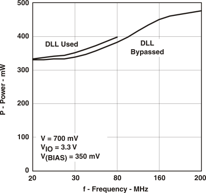 Figure 4-1 Power vs Frequency
Table 4-2 Power for 700-mV DAC Output Compliance + 350-mV Bias at AVDD = 3.3 V, DVDD = 1.8 V, VDD_IO = 1.8 V, VDD_DLL = 3.3 V, 1-MHz Tone on All Channels
| f (MHz) | POWER (mW), DLL BYPASSED |
POWER (mW), DLL USED |
IAVDD (mA) | IDVDD (mA) | IVDD_IO (mA) | IVDD_DLL (mA) |
|---|---|---|---|---|---|---|
| 20 | 328.26 | 331.23 | 93.2 | 10.4 | 1.1 | 0.9 |
| 30 | 336.72 | 349.92 | 93.2 | 15 | 1.2 | 4 |
| 80 | 379.92 | 397.08 | 93.2 | 38.5 | 1.7 | 5.2 |
| 160 | 447.06 | 93.2 | 75.2 | 2.3 | ||
| 200 | 472.26 | 93.2 | 89 | 2.5 |
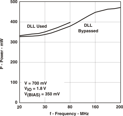 Figure 4-2 Power vs Frequency
Table 4-3 Power for 1.25-V Output Compliance Without Bias at AVDD = 3.3 V, DVDD = 1.8 V, VDD_IO = 3.3 V, VDD_DLL = 3.3 V, 1-MHz Tone on All Channels
| f (MHz) | POWER (mW), DLL BYPASSED |
POWER (mW), DLL USED |
IAVDD (mA) | IDVDD (mA) | IVDD_IO (mA) | IVDD_DLL (mA) |
|---|---|---|---|---|---|---|
| 20 | 556.95 | 559.92 | 162 | 10.4 | 1.1 | 0.9 |
| 30 | 565.56 | 578.76 | 162 | 15 | 1.2 | 4 |
| 80 | 609.51 | 626.67 | 162 | 38.5 | 1.7 | 5.2 |
| 160 | 677.55 | 162 | 75.2 | 2.3 | ||
| 200 | 703.05 | 162 | 89 | 2.5 |
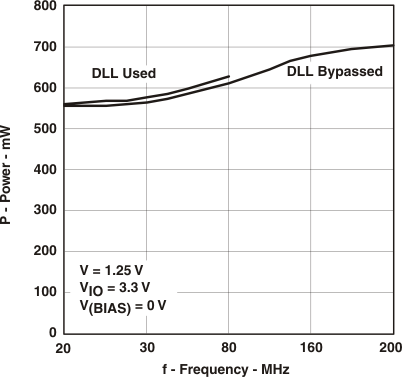 Figure 4-3 Power vs Frequency
Table 4-4 Power for 1.25-V Output Compliance Without Bias at AVDD = 3.3 V, DVDD = 1.8 V, VDD_IO = 1.8 V, VDD_DLL = 3.3 V, 1-MHz Tone on All Channels
| f (MHz) | POWER (mW), DLL BYPASSED |
POWER (mW), DLL USED |
IAVDD (mA) | IDVDD (mA) | IVDD_IO (mA) | IVDD_DLL (mA) |
|---|---|---|---|---|---|---|
| 20 | 555.30 | 558.27 | 162 | 10.4 | 1.1 | 0.9 |
| 30 | 563.76 | 576.96 | 162 | 15 | 1.2 | 4 |
| 80 | 606.96 | 624.12 | 162 | 38.5 | 1.7 | 5.2 |
| 160 | 674.10 | 162 | 75.2 | 2.3 | ||
| 200 | 699.30 | 162 | 89 | 2.5 |
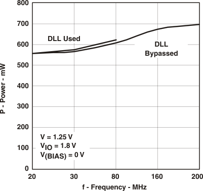 Figure 4-4 Power vs Frequency
4.5 Power Supply
1-MHz FS ramp simultaneously applied to all three channelsover recommended operating conditions with fCLK = 205 MHz, RFS = RFS(nom) (unless otherwise noted)
| PARAMETER | TEST CONDITIONS | MIN | TYP | MAX | UNIT | |||
|---|---|---|---|---|---|---|---|---|
| IAVDD | Operating analog supply current | AVDD = 3.3 V, DVDD = 1.8 V, VDD_DLL = 1.8 V, VDD_IO = 3.3 V, CLK = 80 MHz |
Video + no bias (700 mV) | 94 | 98 | mA | ||
| Video + bias (1.05 V) | 94 | 98 | ||||||
| Generic + no bias (1.25 V) | 162 | 170 | ||||||
| AVDD = 3.3 V, DVDD = 1.8 V, VDD_DLL = 1.8 V (DLL bypassed), VDD_IO = 1.8 V, CLK = 200 MHz |
Video + no bias (700 mV) | 94 | 98 | |||||
| Video + bias (1.05 V) | 94 | 98 | ||||||
| Generic + no bias (1.25 V) | 162 | 170 | ||||||
| IDVDD | Operating digital supply current | AVDD = 3.3 V, DVDD = 1.8 V, VDD_DLL = 1.8 V, VDD_IO = 3.3 V, CLK = 80 MHz |
Video + no bias (700 mV) | 38 | 45 | mA | ||
| Video + bias (1.05 V) | 38 | 45 | ||||||
| Generic + no bias (1.25 V) | 38 | 45 | ||||||
| AVDD = 3.3 V, DVDD = 1.8 V, VDD_DLL = 1.8 V (DLL bypassed), VDD_IO = 1.8 V, CLK = 200 MHz |
Video + no bias (700 mV) | 89 | 95 | |||||
| Video + bias (1.05 V) | 89 | 95 | ||||||
| Generic + no bias (1.25 V) | 89 | 95 | ||||||
| IVDD_IO | Operating I/O supply current | AVDD = 3.3 V, DVDD = 1.8 V, VDD_DLL = 1.8 V, VDD_IO = 3.3 V, CLK = 80 MHz |
Video + no bias (700 mV) | 1.7 | 2.2 | mA | ||
| Video + bias (1.05 V) | 1.7 | 2.2 | ||||||
| Generic + no bias (1.25 V) | 1.7 | 2.2 | ||||||
| AVDD = 3.3 V, DVDD = 1.8 V, VDD_DLL = 1.8 V (DLL bypassed), VDD_IO = 1.8 V, CLK = 200 MHz |
Video + no bias (700 mV) | 1.7 | 2.2 | |||||
| Video + bias (1.05 V) | 1.7 | 2.2 | ||||||
| Generic + no bias (1.25 V) | 1.7 | 2.2 | ||||||
| IVDD_DLL | Operating DLL supply current | AVDD = 3.3 V, DVDD = 1.8 V, VDD_DLL = 1.8 V, VDD_IO = 3.3 V, CLK = 80 MHz |
Video + no bias (700 mV) | 4.9 | 5.6 | mA | ||
| Video + bias (1.05 V) | 4.9 | 5.6 | ||||||
| Generic + no bias (1.25 V) | 4.9 | 5.6 | ||||||
| AVDD = 3.3 V, DVDD = 1.8 V, VDD_DLL = 1.8 V (DLL bypassed), VDD_IO = 1.8 V, CLK = 200 MHz |
Video + no bias (700 mV) | 4.9 | 5.6 | |||||
| Video + bias (1.05 V) | 4.9 | 5.6 | ||||||
| Generic + no bias (1.25 V) | 4.9 | 5.6 | ||||||
| PD | Power disspiation | AVDD = 3.3 V, DVDD = 1.8 V, VDD_DLL = 1.8 V, VDD_IO = 3.3 V, CLK = 80 MHz |
Video + no bias (700 mV) | 398 | 430 | mW | ||
| Video + bias (1.05 V) | 398 | 430 | ||||||
| Generic + no bias (1.25 V) | 641 | 660 | ||||||
| AVDD = 3.3 V, DVDD = 1.8 V, VDD_DLL = 1.8 V (DLL bypassed), VDD_IO = 1.8 V, CLK = 200 MHz |
Video + no bias (700 mV) | 489 | 500 | |||||
| Video + bias (1.05 V) | 489 | 500 | ||||||
| Generic + no bias (1.25 V) | 700 | 735 | ||||||
4.6 Digital Inputs, DC Characteristics
over recommended operating conditions with fCLK = 205 MHz, RFS = RFS(nom) (unless otherwise noted)| PARAMETER | TEST CONDITIONS | MIN | TYP | MAX | UNIT | |
|---|---|---|---|---|---|---|
| IIH | High-level input current | VDD_IO = 3.3 V, Digital inputs and CLK at 0 V for IIL, Digital inputs and CLK at 3.6 V for IIH |
1 | µA | ||
| IIL | Low-level input current | −1 | µA | |||
| IIL(CLK) | Low-level input current, CLK | 1 | µA | |||
| IIH(CLK) | High-level input current, CLK | −1 | µA | |||
| CI | Input capacitance | TA = 25°C | 5 | pF | ||
| ts | GY, RCr, BCb data inputs setup time | VDD_IO = 1.8 V | 1.5 | ns | ||
| VDD_IO = 3.3 V | 1.5 | |||||
| tH | GY, RCr, BCb data inputs hold time | VDD_IO = 1.8 V | 0.5 | ns | ||
| VDD_IO = 3.3 V | 0.5 | |||||
| ts | HS_IN, VS_IN, FID inputs setup time | VDD_IO = 3.3 V (1) | 1.5 | ns | ||
| tH | HS_IN, VS_IN, FID inputs hold time | VDD_IO = 3.3 V (1) | 0.5 | ns | ||
| td(D) | Digital process delay (2) | 10-bit/20-bit 4:2:2 with CSM, CSC, 2x interpolation active | 73 (3) | pixels | ||
| 30-bit 4:4:4 | 33 (3) | |||||
| VESA clock mode (DLL, CSM, CSC, FIRs bypassed) | 9 | |||||
4.7 Analog (DAC) Outputs
over recommended operating conditions with fCLK = 205 MHz, RFS = RFS(nom) (unless otherwise noted)| PARAMETER | TEST CONDITIONS | MIN | TYP | MAX | UNIT | ||
|---|---|---|---|---|---|---|---|
| DAC resolution | 10 (11 bit internal) |
10 (11 bit internal) |
bits | ||||
| INL | Integral nonlinearity | Best-fit VDD_IO = 3.3 V, CLK = 500 kHz |
Video (0.7 + 0.35 V bias) | +0.5/-1.2 | +2/-2 | LSB | |
| Generic (1.25 + 0 V bias) | +1/-2.1 | +5/-5 | |||||
| DNL | Differential nonlinearity | VDD_IO = 3.3 V, CLK = 500 kHz |
Video (0.7 + 0.35 V bias) | +0.2/−0.3 | +1/−1 | LSB | |
| Generic (1.25 + 0 V bias) | +0.3/-0.5 | +1/−1 | |||||
| PSRR | Power supply ripple rejection ratio of DAC output (full scale) | f = dc to 100 kHz (4) | 40 | 42 | dB | ||
| XTALK | Crosstalk between channels (5) | CLK = 205 MHz, -1 dB sine wave applied to active channels, offset bias applied to all channels when turned on, 37.5-Ω load on all channels | 1-MHz sine wave, offset bias off |
49 | dB | ||
| 1-MHz sine wave, offset bias on |
42 | ||||||
| 10-MHz sine wave, offset bias off |
49 | ||||||
| 10-MHz sine wave, offset bias on |
42 | ||||||
| 30-MHz sine wave, offset bias off |
48 | ||||||
| 30-MHz sine wave, offset bias on |
40.5 | ||||||
| KIMBAL | Imbalance between DACs | CLK = 80 MHz (6) | ±2% | ||||
| VOC | DAC output compliance voltage (video only) | RL = 37.5 Ω (7) | Video mode (bias offset can be added) | 0.7 | 0.72 | V | |
| Generic mode (bias offset cannot be added) | 1.25 | 1.3 | |||||
| CO | DAC output capacitance (pin capacitance) | 5 | pF | ||||
| tri | DAC output current rise time | 10 to 90% of full scale, CLK = 80 MHz | 3.5 | 4.2 | ns | ||
| tfi | DAC output current fall time | 10 to 90% of full scale, CLK = 80 MHz | 3.5 | 4.2 | ns | ||
| td | Analog output delay | Measured from falling edge of CLKIN to 50% of full-scale transition (8) | 6.5 | ns | |||
| tsa | Analog output settling time | Measured from 50% of full scale transition on output to output settling, within 2% (9) | 6.6 | ns | |||
| SFDR | Spurious-free dynamic range | 1 MHz, −1 dB FS digital sine input | -55 | dB | |||
| 10 MHz, −1 dB FS digital sine input | -43 | ||||||
| BW | Bandwidth (3 dB) | 90 | MHz | ||||
| Eglitch | Glitch energy | Full-scale code transition at 205 MSPS | 25 | pVs | |||
(1) The HS_IN, VS_IN, and FID input setup and hold times are valid for 3.3-V I/O operation only. These sync inputs are not recommended for use with 1.8-V I/O logic levels.
(2) Defined as the delay on Y pixel data, starting from the rising edge of CLKIN, until the clock period.
(3) CSC contribution: 8 pixels, CSM contribution: 1 pixel, 2x interpolation filter contribution: 18 pixels
(4) PSRR is defined as 20 × log(ripple voltage at DAC output / ripple voltage at AVDD input). Limits from characterization only.
(5) Crosstalk spec applies to each possible pair of the 3 DAC outputs. Limit from characterization only.
(6) The imbalance between DACs applies to all possible pairs of the three DACs.
(7) Nominal values at RFS = RFS(nom). Limit from characterization only. Excludes bias offset.
(8) This value excludes the digital process delay, tD(D). Limit from characterization only. Data is clocked in on the rising edge of CLKIN. Analog outputs become available on the falling edge of CLKIN.
(9) Limit from characterization only.
4.8 Nonlinearity
4.8.1 Differential Nonlinearity (DNL) and Integral Nonlinearity (INL) for 700 mV Without Bias
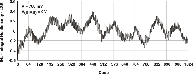 Figure 4-5 Integral Nonlinearity vs Code
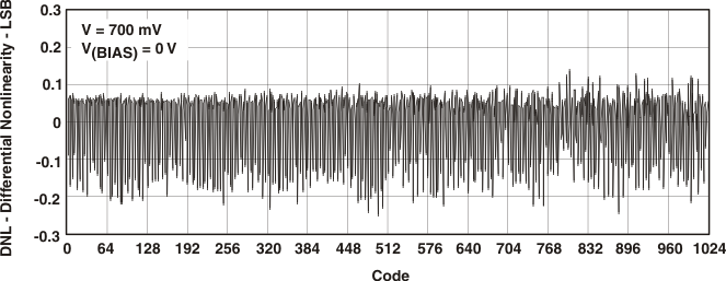 Figure 4-6 Differential Nonlinearity vs Code
4.8.2 Differential Nonlinearity (DNL) and Integral Nonlinearity (INL) for 700 mV + 350-mV Bias
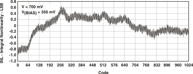 Figure 4-7 Integral Nonlinearity vs Code
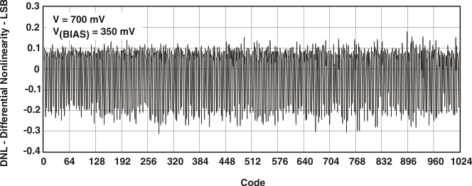 Figure 4-8 Differential Nonlinearity vs Code
4.8.3 Differential Nonlinearity (DNL) and Integral Nonlinearity (INL) for 1.25 V Without Bias
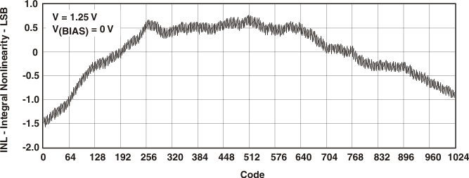 Figure 4-9 Integral Nonlinearity vs Code
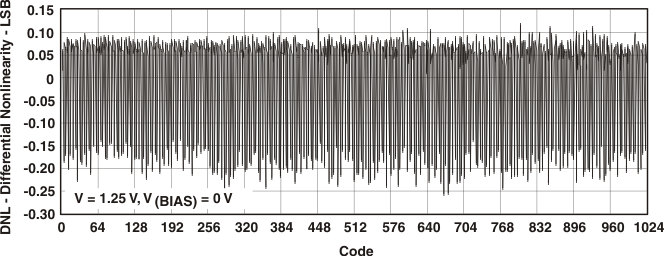 Figure 4-10 Differential Nonlinearity vs Code
4.9 Analog Output Bandwidth (sinx/x corrected) at fS = 205 MSPS
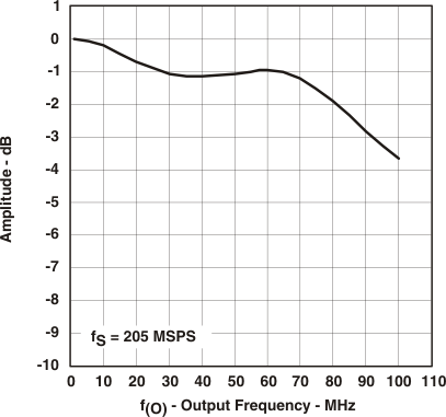 Figure 4-11 Amplitude vs Output Frequency
4.10 Output Compliance vs Full-Scale Adjustment Resistor Value
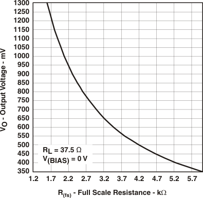 Figure 4-12 Output Voltage vs Full-Scale Resistance
4.11 Vertical Sync of the HDTV 1080I Format Preset in First and Second Field, and Horizontal Line Waveform Detail
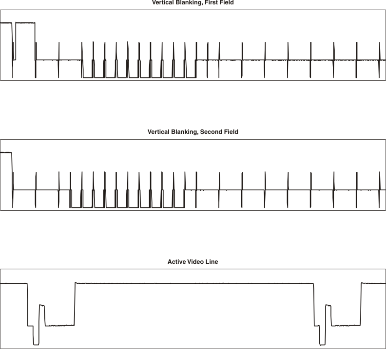 Figure 4-13 THS8200 Output Waveforms for 1080I: Vertical Blanking in First and Second Fields, and Active Video