SLLSEY3E May 2018 – May 2019 THVD1410 , THVD1450 , THVD1451 , THVD1452
PRODUCTION DATA.
- 1 Features
- 2 Applications
- 3 Description
- 4 Revision History
- 5 Device Comparison Table
- 6 Pin Configuration and Functions
-
7 Specifications
- 7.1 Absolute Maximum Ratings
- 7.2 ESD Ratings
- 7.3 ESD Ratings [IEC]
- 7.4 Recommended Operating Conditions
- 7.5 Thermal Information
- 7.6 Power Dissipation
- 7.7 Electrical Characteristics
- 7.8 Switching Characteristics
- 7.9 Typical Characteristics: All Devices
- 7.10 Typical Characteristics: THD1450, THVD1451 and THVD1452
- 7.11 Typical Characteristics: THVD1410
- 8 Parameter Measurement Information
- 9 Detailed Description
- 10Application and Implementation
- 11Power Supply Recommendations
- 12Layout
- 13Device and Documentation Support
- 14Mechanical, Packaging, and Orderable Information
Package Options
Refer to the PDF data sheet for device specific package drawings
Mechanical Data (Package|Pins)
- D|8
- DGK|8
- DRB|8
Thermal pad, mechanical data (Package|Pins)
- DRB|8
Orderable Information
10.2 Typical Application
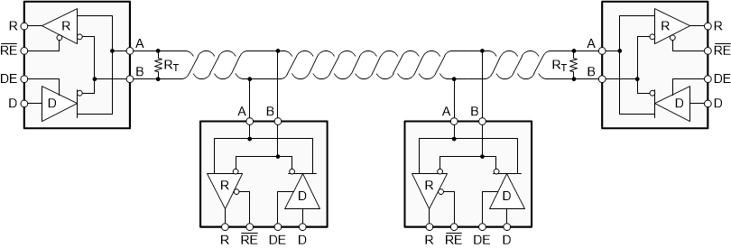
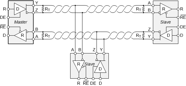
An RS-485 bus consists of multiple transceivers connecting in parallel to a bus cable. To eliminate line reflections, each cable end is terminated with a termination resistor, RT, whose value matches the characteristic impedance, Z0, of the cable. This method, known as parallel termination, generally allows for higher data rates over longer cable length.
 Figure 31. Typical RS-485 Network With Half-Duplex Transceivers
  Figure 32. Typical RS-485 Network With Full-Duplex Transceivers