SLLSEV5D July 2017 – June 2019 TIOL111 , TIOL1113 , TIOL1115
PRODUCTION DATA.
- 1 Features
- 2 Applications
- 3 Description
- 4 Revision History
- 5 Pin Configuration and Functions
- 6 Specifications
- 7 Parameter Measurement Information
-
8 Detailed Description
- 8.1 Overview
- 8.2 Functional Block Diagrams
- 8.3
Feature Description
- 8.3.1 Wake Up Detection
- 8.3.2 Current Limit Configuration
- 8.3.3 Current Fault Detection, Indication and Auto Recovery
- 8.3.4 Thermal Warning, Thermal Shutdown
- 8.3.5 Fault Reporting (NFAULT)
- 8.3.6 Transceiver Function Tables
- 8.3.7 The Integrated Voltage Regulator (LDO)
- 8.3.8 Reverse Polarity Protection
- 8.3.9 Integrated Surge Protection and Transient Waveform Tolerance
- 8.3.10 Power Up Sequence (TIOL111)
- 8.3.11 Undervoltage Lock-Out (UVLO)
- 8.4 Device Functional Modes
- 9 Application and Implementation
- 10Power Supply Recommendations
- 11Layout
- 12Device and Documentation Support
- 13Mechanical, Packaging, and Orderable Information
Package Options
Mechanical Data (Package|Pins)
- DMW|10
Thermal pad, mechanical data (Package|Pins)
Orderable Information
7 Parameter Measurement Information
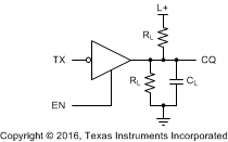
 Figure 6. Test Circuit for Driver Switching
  Figure 7. Waveforms for Driver Output Switching Measurements
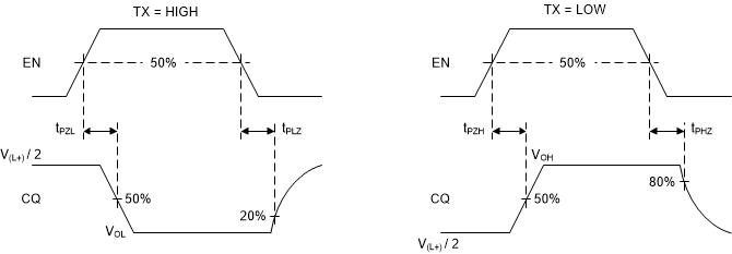
  Figure 8. Waveforms for Driver Enable/Disable Time Measurements
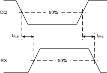
  Figure 9. Receiver Switching Measurements
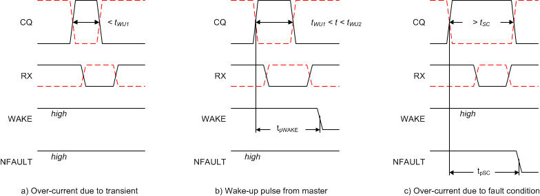
  Figure 10. Overcurrent and Wake Conditions for EN = H, TX = H (Full Lines);
and TX = L (Red Dotted Lines)