SLOS437R April   2004  – April 2024 TL103W , TL103WA , TL103WB

PRODUCTION DATA  

  1.   1
  2. Features
  3. Applications
  4. Description
  5. Pin Configuration and Functions
  6. Specifications
    1. 5.1 Absolute Maximum Ratings
    2. 5.2 ESD Ratings
    3. 5.3 Recommended Operating Conditions
    4. 5.4 Thermal Information
    5. 5.5 Electrical Characteristics: OP AMP1 (VREF at Noninverting input)
    6. 5.6 Electrical Characteristics: OP AMP2 (Independent Amplifier)
    7. 5.7 Typical Characteristics: TL103WB
  7. Detailed Description
    1. 6.1 Overview
    2. 6.2 Functional Block Diagram
    3. 6.3 Feature Description
      1. 6.3.1 Internal Reference
      2. 6.3.2 Input Common Mode Range
      3. 6.3.3 EMI Rejection
    4. 6.4 Device Functional Modes
  8. Application and Implementation
    1. 7.1 Application Information
    2. 7.2 Typical Applications
      1. 7.2.1 Isolated Flyback CC/CV Feedback
        1. 7.2.1.1 Design Requirements
        2. 7.2.1.2 Detailed Design Procedure
          1. 7.2.1.2.1 Constant Current Circuit
          2. 7.2.1.2.2 Constant Voltage Circuit
      2. 7.2.2 Constant Current Sink
    3. 7.3 Power Supply Recommendations
    4. 7.4 Layout
      1. 7.4.1 Layout Guidelines
      2. 7.4.2 Layout Example
  9. Device and Documentation Support
    1. 8.1 Documentation Support
      1. 8.1.1 Related Documentation
    2. 8.2 Receiving Notification of Documentation Updates
    3. 8.3 Support Resources
    4. 8.4 Trademarks
    5. 8.5 Electrostatic Discharge Caution
    6. 8.6 Glossary
  10. Revision History
  11. 10Mechanical, Packaging, and Orderable Information

Package Options

Refer to the PDF data sheet for device specific package drawings

Mechanical Data (Package|Pins)
  • D|8
Thermal pad, mechanical data (Package|Pins)
Orderable Information

Pin Configuration and Functions

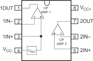
GUID-498CBD37-B181-4ADE-A53D-B2B1FBA10930-low.gifFigure 4-1 D and DDF Packages,
8-Pin SOIC and SOT-23-THN
(Top View)
Table 4-1 Pin Functions
PIN TYPE(1) DESCRIPTION
NAME NO.
1OUT 1 O Opamp 1 output
1IN– 2 I Opamp 1 inverting input
1IN+ 3 I Opamp 1 non-inverting input and Shunt reference cathode terminal
VCC– 4 I Negative Supply Voltage
2IN+ 5 I Opamp 2 non-inverting input
2IN– 6 I Opamp 2 inverting input
2OUT 7 O Opamp 2 output
VCC+ 8 I Positive Supply Voltage
I = input, O = output