SLVS581B September 2006 – June 2015 TL5209
PRODUCTION DATA.
- 1 Features
- 2 Applications
- 3 Description
- 4 Typical Application Schematic
- 5 Revision History
- 6 Pin Configuration and Functions
- 7 Specifications
- 8 Detailed Description
- 9 Application and Implementation
- 10Power Supply Recommendations
- 11Layout
- 12Device and Documentation Support
- 13Mechanical, Packaging, and Orderable Information
Package Options
Refer to the PDF data sheet for device specific package drawings
Mechanical Data (Package|Pins)
- D|8
Thermal pad, mechanical data (Package|Pins)
Orderable Information
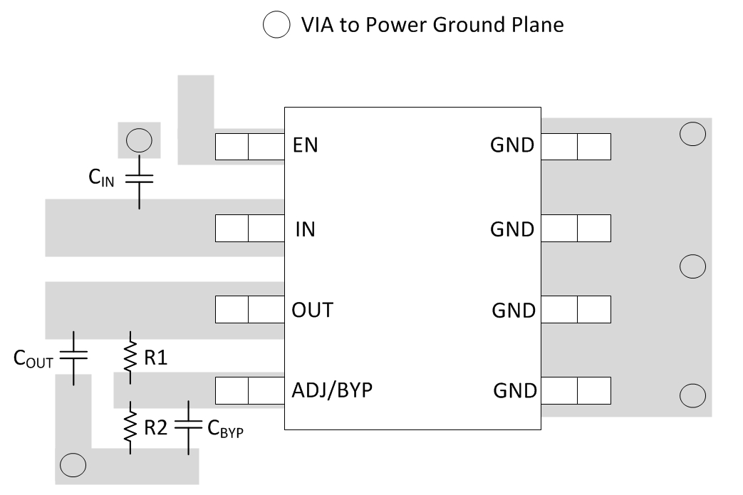
11 Layout
11.1 Layout Guidelines
For best performance, VIN, VOUT, and GND traces must be as short and wide as possible to help minimize the parasitic electrical effects. To be most effective, the input and output capacitors must be placed close to the device to minimize the effects that parasitic trace inductances may have on normal operation.
11.2 Layout Example
 Figure 42. TL5209 Layout Schematic