SLVS581B September 2006 – June 2015 TL5209
PRODUCTION DATA.
- 1 Features
- 2 Applications
- 3 Description
- 4 Typical Application Schematic
- 5 Revision History
- 6 Pin Configuration and Functions
- 7 Specifications
- 8 Detailed Description
- 9 Application and Implementation
- 10Power Supply Recommendations
- 11Layout
- 12Device and Documentation Support
- 13Mechanical, Packaging, and Orderable Information
Package Options
Refer to the PDF data sheet for device specific package drawings
Mechanical Data (Package|Pins)
- D|8
Thermal pad, mechanical data (Package|Pins)
Orderable Information
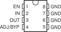
6 Pin Configuration and Functions
D Package
8-Pin SOIC
Top View

Pin Functions
| PIN | I/O | DESCRIPTION | |
|---|---|---|---|
| NAME | NO. | ||
| ADJ/BYP | 4 | I | Adjust/Bypass pin, forces a constant voltage of 1.242 V to allow for adjusting the output voltage with external resistors. A bypass capacitance can be used on this pin to slow down the ramp up of the output voltage. |
| EN | 1 | I | Control input, active high |
| GND | 5-8 | - | Ground |
| IN | 2 | I | Input voltage |
| OUT | 3 | O | Output voltage |