SLVS036N September 1981 – January 2015 TL783
PRODUCTION DATA.
- 1 Features
- 2 Applications
- 3 Description
- 4 Simplified Schematic
- 5 Revision History
- 6 Pin Configuration and Functions
- 7 Specifications
- 8 Detailed Description
- 9 Application and Implementation
- 10Power Supply Recommendations
- 11Layout
- 12Device and Documentation Support
- 13Mechanical, Packaging, and Orderable Information
Package Options
Mechanical Data (Package|Pins)
- KCS|3
Thermal pad, mechanical data (Package|Pins)
Orderable Information
9 Application and Implementation
NOTE
Information in the following applications sections is not part of the TI component specification, and TI does not warrant its accuracy or completeness. TI’s customers are responsible for determining suitability of components for their purposes. Customers should validate and test their design implementation to confirm system functionality.
9.1 Application Information
9.1.1 General Configurations
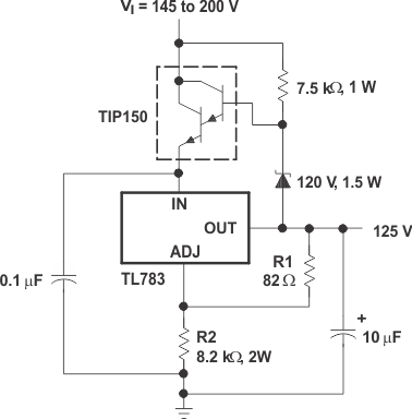 Figure 13. 125-V Short-Circuit-Protected Off-Line Regulator
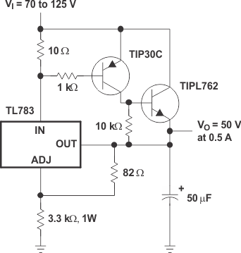 Figure 14. 50-V Regulator With Current Boost
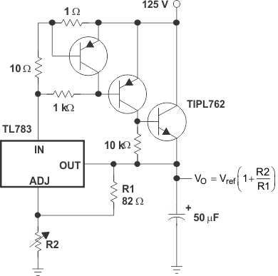 Figure 15. Adjustable Regulator With Current Boost and Current Limit
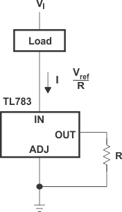 Figure 16. Current-Sinking Regulator
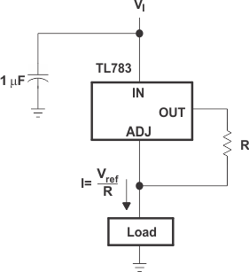 Figure 17. Current-Sourcing Regulator
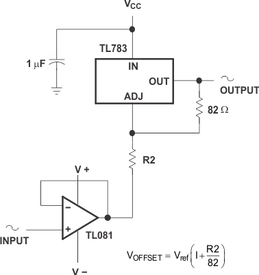 Figure 18. High-Voltage Unity-Gain Offset Amplifier
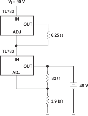 Figure 19. 48-V 200-mA Float Charger
9.2 Typical Application
The TL783 is typically used as an adjustable regulator.
9.2.1 Design Requirements
- Input and output decoupling capacitors for noise filtering.
- Resistor divider consisting of R1 and R2 to set the output voltage.
9.2.2 Detailed Design Procedure
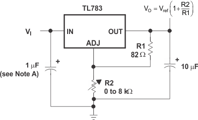
The internal reference (see Simplified Schematic) generates 1.25 V nominal (Vref) between OUT and ADJ. This voltage is developed across R1 and causes a constant current to flow through R1 and the programming resistor R2, giving an output voltage of:
VO = Vref (1 + R2 / R1) + lI(ADJ) (R2)
or
VO ≉ Vref (1 + R2 / R1)
The TL783 was designed to minimize the input current at ADJ and maintain consistency over line and load variations, thereby minimizing the associated (R2) error term.
To maintain II(ADJ) at a low level, all quiescent operating current is returned to the output terminal. This quiescent current must be sunk by the external load and is the minimum load current necessary to prevent the output from rising. The recommended R1 value of 82 Ω provides a minimum load current of 15 mA. Larger values can be used when the input-to-output differential voltage is less than 125 V (see the output-current curve in Figure 12) or when the load sinks some portion of the minimum current.
9.2.2.1 Bypass Capacitors
The TL783 regulator is stable without bypass capacitors; however, any regulator becomes unstable with certain values of output capacitance if an input capacitor is not used. Therefore, the use of input bypassing is recommended whenever the regulator is located more than four inches from the power-supply filter capacitor. A 1-μF tantalum or aluminum electrolytic capacitor usually is sufficient.
Adjustment-terminal capacitors are not recommended for use on the TL783 because they can seriously degrade load transient response, as well as create a need for extra protection circuitry. Excellent ripple rejection presently is achieved without this added capacitor.
Due to the relatively low gain of the MOS output stage, output voltage dropout may occur under large-load transient conditions. The addition of an output bypass capacitor greatly enhances load transient response and prevents dropout. For most applications, it is recommended that an output bypass capacitor be used, with a minimum value of:
Co (μF) = 15 / VO
Larger values provide proportionally better transient-response characteristics.
9.2.2.2 Protection Circuitry
The TL783 regulator includes built-in protection circuits capable of guarding the device against most overload conditions encountered in normal operation. These protective features are current limiting, safe-operating-area protection, and thermal shutdown. These circuits protect the device under occasional fault conditions only. Continuous operation in the current limit or thermal shutdown mode is not recommended.
The internal protection circuits of the TL783 protect the device up to maximum-rated VI as long as certain precautions are taken. If Vl is switched on instantaneously, transients exceeding maximum input ratings may occur, which can destroy the regulator. Usually, these are caused by lead inductance and bypass capacitors causing a ringing voltage on the input. In addition, when rise times in excess of 10 V/ns are applied to the input, a parasitic npn transistor in parallel with the DMOS output can be turned on, causing the device to fail. If the device is operated over 50 V and the input is switched on, rather than ramped on, a low-Q capacitor, such as tantalum or aluminum electrolytic, should be used, rather than ceramic, paper, or plastic bypass capacitors. A Q factor of 0.015, or greater, usually provides adequate damping to suppress ringing. Normally, no problems occur if the input voltage is allowed to ramp upward through the action of an ac line rectifier and filter network.
Similarly, when an instantaneous short circuit is applied to the output, both ringing and excessive fall times can result. A tantalum or aluminum electrolytic bypass capacitor is recommended to eliminate this problem. However, if a large output capacitor is used, and the input is shorted, addition of a protection diode may be necessary to prevent capacitor discharge through the regulator. The amount of discharge current delivered is dependent on output voltage, size of capacitor, and fall time of Vl. A protective diode (see Figure 21) is required only for capacitance values greater than:
Co (μF) = 3 × 10⁴ / (VO)2
Care always should be taken to prevent insertion of regulators into a socket with power on. Power should be turned off before removing or inserting regulators.
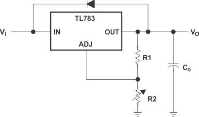 Figure 21. Regulator With Protective Diode
9.2.2.3 Load Regulation
The current-set resistor (R1) should be located close to the regulator output terminal, rather than near the load. This eliminates long line drops from being amplified, through the action of R1 and R2, to degrade load regulation. To provide remote ground sensing, R2 should be near the load ground.
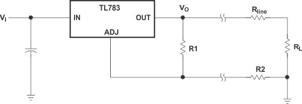 Figure 22. Regulator With Current-Set Resistor
9.2.3 Application Curves
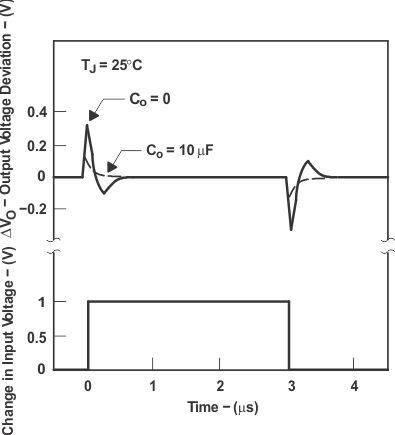 Figure 23. Line Transient Response
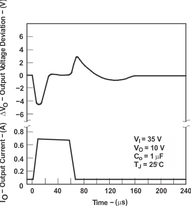 Figure 24. Load Transient Response