SLVS036N September 1981 – January 2015 TL783
PRODUCTION DATA.
- 1 Features
- 2 Applications
- 3 Description
- 4 Simplified Schematic
- 5 Revision History
- 6 Pin Configuration and Functions
- 7 Specifications
- 8 Detailed Description
- 9 Application and Implementation
- 10Power Supply Recommendations
- 11Layout
- 12Device and Documentation Support
- 13Mechanical, Packaging, and Orderable Information
Package Options
Mechanical Data (Package|Pins)
- KCS|3
Thermal pad, mechanical data (Package|Pins)
Orderable Information
7 Specifications
7.1 Absolute Maximum Ratings
over operating temperature range (unless otherwise noted)(1)| MIN | MAX | UNIT | |||
|---|---|---|---|---|---|
| Vl – VO | Input-to-output differential voltage | 125 | V | ||
| TJ | Operating virtual junction temperature | 150 | °C | ||
| Tstg | Storage temperature range | –65 | 150 | °C | |
(1) Stresses beyond those listed under Absolute Maximum Ratings may cause permanent damage to the device. These are stress ratings only, and functional operation of the device at these or any other conditions beyond those indicated under Recommended Operating Conditions is not implied. Exposure to absolute-maximum-rated conditions for extended periods may affect device reliability.
7.2 ESD Ratings
| VALUE | UNIT | |||
|---|---|---|---|---|
| V(ESD) | Electrostatic discharge | Human body model (HBM), per ANSI/ESDA/JEDEC JS-001, all pins(1) | 2500 | V |
| Charged device model (CDM), per JEDEC specification JESD22-C101, all pins(2) | 1000 | |||
(1) JEDEC document JEP155 states that 500-V HBM allows safe manufacturing with a standard ESD control process.
(2) JEDEC document JEP157 states that 250-V CDM allows safe manufacturing with a standard ESD control process.
7.3 Recommended Operating Conditions
| MIN | MAX | UNIT | |||
|---|---|---|---|---|---|
| Vl – VO | Input-to-output differential voltage | 125 | V | ||
| IO | Output current | 15 | 700 | mA | |
| TJ | Operating virtual junction temperature | 0 | 125 | °C | |
7.4 Thermal Information
| THERMAL METRIC(1) | TL783 | UNIT | |||
|---|---|---|---|---|---|
| KTE | KTT | KC | |||
| 3 PINS | |||||
| RθJA | Junction-to-ambient thermal resistance | 23 | 25.3 | 19 | °C/W |
| RθJC(top) | Junction-to-case (top) thermal resistance | N/A | 18 | 17 | |
| RθJP | Junction-to-exposed-pad thermal resistance | 2.7 | 1.94 | 3 | |
(1) For more information about traditional and new thermal metrics, see the IC Package Thermal Metrics application report, SPRA953.
7.5 Electrical Characteristics
Vl – VO = 25 V, IO = 0.5 A, TJ = 0°C to 125°C (unless otherwise noted)| PARAMETER | TEST CONDITIONS(1) | MIN | TYP | MAX | UNIT | |
|---|---|---|---|---|---|---|
| Input voltage regulation(2) | Vl – VO = 20 V to 125 V, P ≤ rated dissipation | TJ = 25°C | 0.001 | 0.01 | %/V | |
| TJ = 0°C to 125°C | 0.004 | 0.02 | ||||
| Ripple rejection | ΔVI(PP) = 10 V, VO = 10 V, f = 120 Hz | 66 | 76 | dB | ||
| Output voltage regulation | IO = 15 mA to 700 mA, TJ = 25°C | VO ≤ 5 V | 7.5 | 25 | mV | |
| VO ≥ 5 V | 0.15% | 0.5% | — | |||
| IO = 15 mA to 700 mA, P ≤ rated dissipation | VO ≤ 5 V | 20 | 70 | mV | ||
| VO ≥ 5 V | 0.3% | 1.5% | — | |||
| Output voltage change with temperature | 0.4% | |||||
| Output voltage long-term drift | 1000 hours at TJ = 125°C, Vl – VO = 125 V | 0.2% | ||||
| Output noise voltage | f = 10 Hz to 10 kHz, TJ = 25°C | 0.003% | ||||
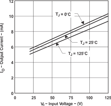
| Minimum output current to maintain regulation | Vl – VO = 125 V | 15 | mA | |||
| Peak output current | Vl – VO = 25 V, t = 1 ms | 1100 | mA | |||
| Vl – VO = 15 V, t = 30 ms | 715 | |||||
| Vl – VO = 25 V, t = 30 ms | 700 | 900 | ||||
| Vl – VO = 125 V, t = 30 ms | 100 | 250 | ||||
| ADJ input current | 83 | 110 | μA | |||
| Change in ADJ input current | Vl – VO = 15 V to 125 V, IO = 15 mA to 700 mA, P ≤ rated dissipation | 0.5 | 5 | μA | ||
| Reference voltage (OUT to ADJ)(3) | Vl – VO = 10 V to 125 V, IO = 15 mA to 700 mA, P ≤ rated dissipation | 1.2 | 1.27 | 1.3 | V | |
(1) Pulse-testing techniques maintain the junction temperature as close to the ambient temperature as possible. Thermal effects must be taken into account separately.
(2) Input voltage regulation is expressed here as the percentage change in output voltage per 1-V change at the input
(3) Due to the dropout voltage and output current-limiting characteristics of this device, output current is limited to less than 700 mA at input-to-output voltage differentials of less than 25 V.
7.6 Typical Characteristics
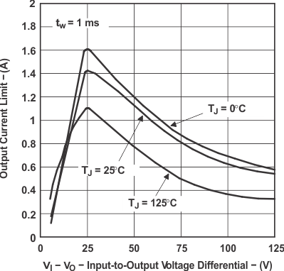 Figure 1. Output Current Limit
 vs
Input-to-Output Voltage Differential
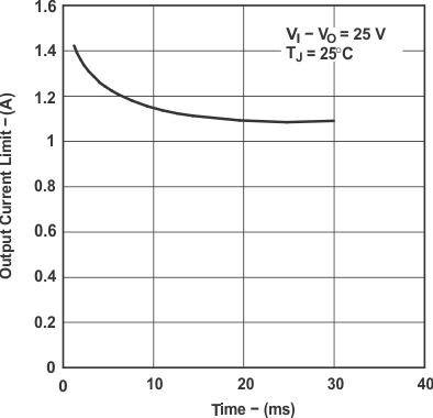 Figure 3. Output Current Limit
vs
Time
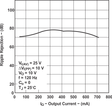 Figure 5. Ripple Rejection
vs
Output Current
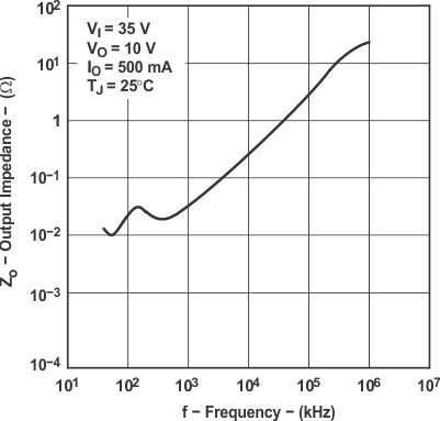 Figure 7. Output Impedance
vs
Frequency
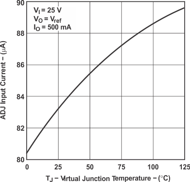 Figure 9. Input Current at ADJ
 vs
Virtual Junction Temperature
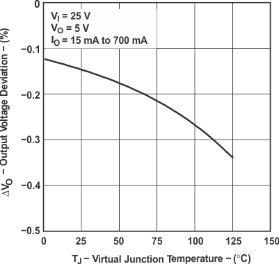 Figure 11. Output Voltage Deviation
vs
Virtual Junction Temperature
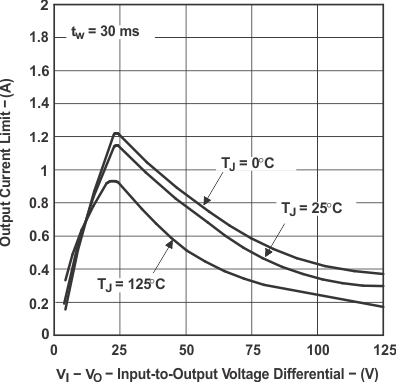 Figure 2. Output Current Limit
 vs
Input-to-Output Voltage Differential
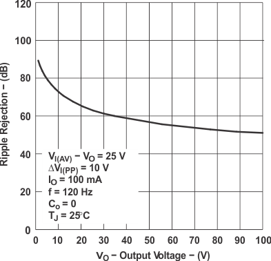 Figure 4. Ripple Rejection
vs
Output Voltage
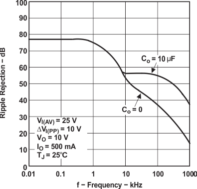 Figure 6. Ripple Rejection
vs
Frequency
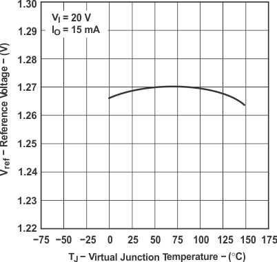 Figure 8. Reference Voltage
vs
Virtual Junction Temperature
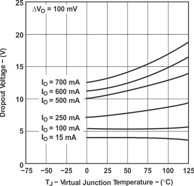 Figure 10. Dropout Voltage
 vs
Virtual Junction Temperature