SLOS510E September 2006 – October 2016 TLC082-Q1 , TLC084-Q1
PRODUCTION DATA.
- 1 Features
- 2 Applications
- 3 Description
- 4 Revision History
- 5 Pin Configuration and Functions
-
6 Specifications
- 6.1 Absolute Maximum Ratings
- 6.2 ESD Ratings
- 6.3 Recommended Operating Conditions
- 6.4 Thermal Information
- 6.5 Electrical Characteristics: VDD = 5 V
- 6.6 Electrical Characteristics: VDD = 12 V
- 6.7 Operating Characteristics: VDD = 5 V
- 6.8 Operating Characteristics: VDD = 12 V
- 6.9 Typical Characteristics
- 7 Parameter Measurement Information
- 8 Detailed Description
- 9 Application and Implementation
- 10Power Supply Recommendations
- 11Layout
- 12Device and Documentation Support
- 13Mechanical, Packaging, and Orderable Information
Package Options
Mechanical Data (Package|Pins)
- PWP|20
Thermal pad, mechanical data (Package|Pins)
- PWP|20
Orderable Information
8 Detailed Description
8.1 Overview
The TLC08x-Q1 BiCMOS amplifiers provide an upgrade path for BiFET users who are moving away from dual-supply to single-supply systems and demand higher AC and DC performance. With performance rated from 4.5 V to 16 V across an automotive temperature range (–40°C to 125°C), BiMOS suits a wide range of audio, automotive, industrial, and instrumentation applications. BiCMOS amplifiers combine a very high input low-noise CMOS front end drive bipolar output stage, thus providing the optimum performance features of both. AC performance include a bandwidth of 10 MHz and voltage noise of 8.5 nV/√Hz.
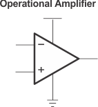
8.2 Functional Block Diagram

8.3 Feature Description
The TLC08x-Q1 family features 10-MHz bandwidth and voltage noise of 8.5 nV/√Hz with performance rated from 4.5 V to 16 V across an automotive temperature range (–40°C to 125°C). BiMOS suits a wide range of audio, automotive, industrial, and instrumentation applications.
8.4 Device Functional Modes
The TLC08x-Q1 family of devices is powered on when the supply is connected. The device can operate with single or dual supply, depending on the application. The device is in its full performance once the supply is above the recommended value.
8.5 Programming
8.5.1 Macromodel Information
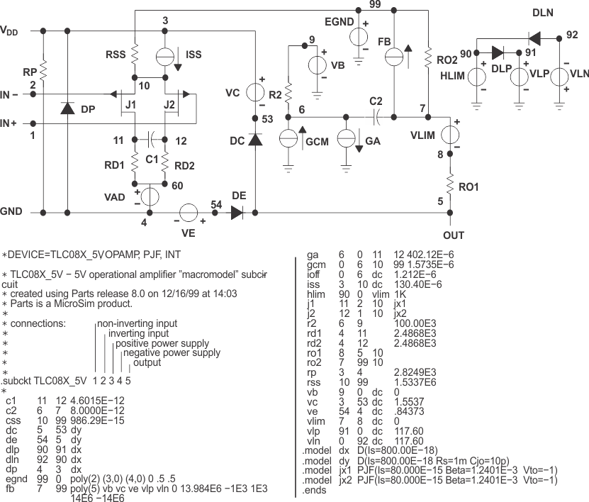
Derivation of the provided macromodel information was by use of Microsim Parts™, the model generation software used with Microsim PSpice™. The Boyle macromodel (1) and subcircuit in Figure 38 are generated using the TLC08x-Q1 typical electrical and operating characteristics at TA = 25°C. Using this information, output simulations of the following key parameters can be generated to a tolerance of 20% (in most cases):
- Maximum positive output voltage swing
- Maximum negative output voltage swing
- Slew rate
- Quiescent power dissipation
- Input bias current
- Open-loop voltage amplification
- Unity-gain frequency
- Common-mode rejection ratio
- Phase margin
- DC output resistance
- AC output resistance
- Short-circuit output current limit
 Figure 38. Boyle Macromodel and Subcircuit