SLOS190H February 1997 – March 2016 TLC2272 , TLC2272A , TLC2272AM , TLC2272M , TLC2274 , TLC2274A , TLC2274AM , TLC2274M
PRODUCTION DATA.
- 1 Features
- 2 Applications
- 3 Description
- 4 Revision History
- 5 Pin Configuration and Functions
-
6 Specifications
- 6.1 Absolute Maximum Ratings
- 6.2 ESD Ratings
- 6.3 Recommended Operating Conditions
- 6.4 Thermal Information
- 6.5 TLC2272 and TLC2272A Electrical Characteristics VDD = 5 V
- 6.6 TLC2272 and TLC2272A Electrical Characteristics VDD± = ±5 V
- 6.7 TLC2274 and TLC2274A Electrical Characteristics VDD = 5 V
- 6.8 TLC2274 and TLC2274A Electrical Characteristics VDD± = ±5 V
- 6.9 Typical Characteristics
- 7 Detailed Description
- 8 Application and Implementation
- 9 Power Supply Recommendations
- 10Layout
- 11Device and Documentation Support
- 12Mechanical, Packaging, and Orderable Information
Package Options
Mechanical Data (Package|Pins)
Thermal pad, mechanical data (Package|Pins)
- PS|8
Orderable Information
1 Features
- Output Swing Includes Both Supply Rails
- Low Noise: 9 nV/√Hz Typical at f = 1 kHz
- Low-Input Bias Current: 1-pA Typical
- Fully-Specified for Both Single-Supply and Split-Supply Operation
- Common-Mode Input Voltage Range Includes Negative Rail
- High-Gain Bandwidth: 2.2-MHz Typical
- High Slew Rate: 3.6-V/μs Typical
- Low Input Offset Voltage: 950 μV Maximum at TA = 25°C
- Macromodel Included
- Performance Upgrades for the TLC272 and TLC274
- Available in Q-Temp Automotive
2 Applications
- White Goods (Refrigerators, Washing Machines)
- Hand-held Monitoring Systems
- Configuration Control and Print Support
- Transducer Interfaces
- Battery-Powered Applications
3 Description
The TLC2272 and TLC2274 are dual and quadruple operational amplifiers from Texas Instruments. Both devices exhibit rail-to-rail output performance for increased dynamic range in single- or split-supply applications. The TLC227x family offers 2 MHz of bandwidth and 3 V/μs of slew rate for higher-speed applications. These devices offer comparable AC performance while having better noise, input offset voltage, and power dissipation than existing CMOS operational amplifiers. The TLC227x has a noise voltage of 9 nV/√Hz, two times lower than competitive solutions.
The TLC227x family of devices, exhibiting high input impedance and low noise, is excellent for small-signal conditioning for high-impedance sources such as piezoelectric transducers. Because of the micropower dissipation levels, these devices work well in hand-held monitoring and remote-sensing applications. In addition, the rail-to-rail output feature, with single- or split-supplies, makes this family a great choice when interfacing with analog-to-digital converters (ADCs). For precision applications, the TLC227xA family is available with a maximum input offset voltage of 950 μV. This family is fully characterized at 5 V and ±5 V.
The TLC227x also make great upgrades to the TLC27x in standard designs. They offer increased output dynamic range, lower noise voltage, and lower input offset voltage. This enhanced feature set allows them to be used in a wider range of applications. For applications that require higher output drive and wider input voltage range, see the TLV2432 and TLV2442 devices.
If the design requires single amplifiers, see the TLV2211, TLV2221 and TLV2231 family. These devices are single rail-to-rail operational amplifiers in the SOT-23 package. Their small size and low power consumption make them ideal for high density, battery-powered equipment.
Device Information(1)
| PART NUMBER | PACKAGE | BODY SIZE (NOM) |
|---|---|---|
| TLC2272 | TSSOP (8) | 4.40 mm × 3.00 mm |
| SOIC (8) | 3.91 mm × 4.90 mm | |
| SO (8) | 5.30 mm × 6.20 mm | |
| PDIP (8) | 6.35 mm × 9.81 mm | |
| TLC2274 | TSSOP (14) | 4.40 mm × 5.00 mm |
| SOIC (14) | 3.91 mm × 8.65 mm | |
| SO (14) | 5.30 mm × 10.30 mm | |
| PDIP (14) | 6.35 mm × 19.30 mm |
- For all available packages, see the orderable addendum at the end of the data sheet.
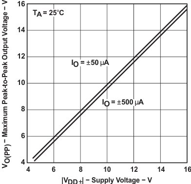
Maximum Peak-to-Peak Output Voltage vs
Supply Voltage

4 Revision History
Changes from G Revision (May 2004) to H Revision
- Added Feature Description section, Device Functional Modes, Application and Implementation section, Power Supply Recommendations section, Layout section, Device and Documentation Supportsection, and Mechanical, Packaging, and Orderable Information section.Go
- Added ESD Rating table for the D and PW package devices. Go