SGLS156F March 2003 – December 2016 TLC3702-Q1
PRODUCTION DATA.
- 1 Features
- 2 Applications
- 3 Description
- 4 Revision History
- 5 Pin Configuration and Functions
- 6 Specifications
- 7 Parameter Measurement Information
- 8 Detailed Description
- 9 Application and Implementation
- 10Power Supply Recommendations
- 11Layout
- 12Device and Documentation Support
- 13Mechanical, Packaging, and Orderable Information
Package Options
Refer to the PDF data sheet for device specific package drawings
Mechanical Data (Package|Pins)
- D|8
- PW|8
Thermal pad, mechanical data (Package|Pins)
Orderable Information
9 Application and Implementation
NOTE
Information in the following applications sections is not part of the TI component specification, and TI does not warrant its accuracy or completeness. TI’s customers are responsible for determining suitability of components for their purposes. Customers should validate and test their design implementation to confirm system functionality.
9.1 Application Information
The inputs should always remain within the supply rails to avoid forward biasing the diodes in the electrostatic discharge (ESD) protection structure. If either input exceeds this range, the device is not damaged as long as the input is limited to less than 5 mA. To maintain the expected output state, the inputs must remain within the common-mode range. For example, at 25°C with VDD = 5 V, both inputs must remain between –0.2 V and 4 V to ensure proper device operation.
To ensure reliable operation, the supply should be decoupled with a capacitor (0.1 µF) that is positioned as close to the device as possible.
The TLC3702-Q1 has internal ESD-protection circuits that prevent functional failures at voltages up to 2000 V as tested under MIL-STD-883C, Method 3015.2; however, care should be exercised in handling these devices as exposure to ESD may result in the degradation of the device parametric performance.
9.2 Typical Applications
9.2.1 Achieving Greater Noise Immunity
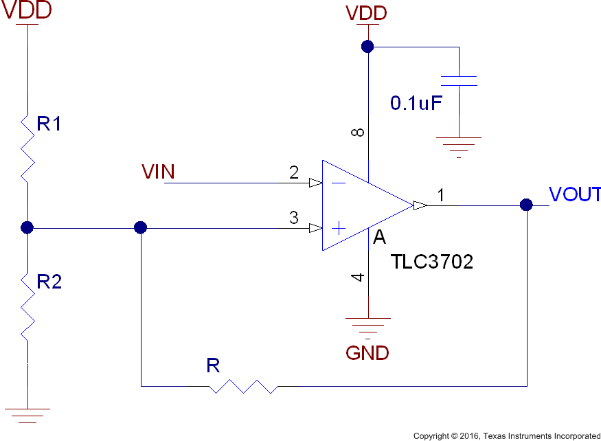
 Figure 25. Application Adding Hysteresis to the TLC3702-Q1
9.2.1.1 Design Requirements
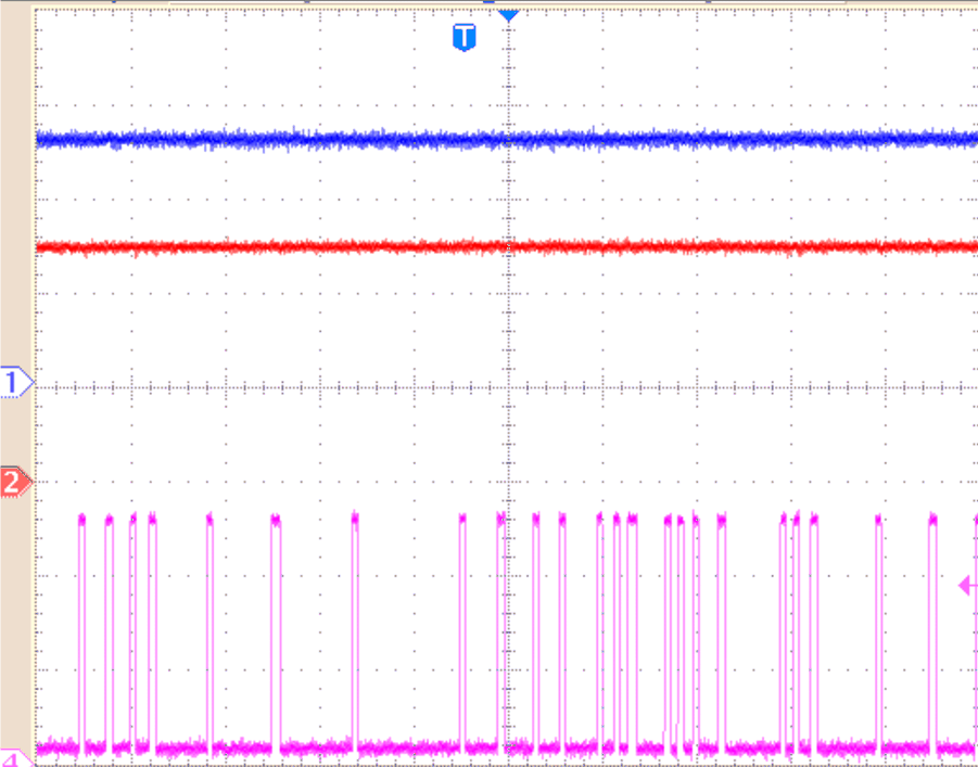
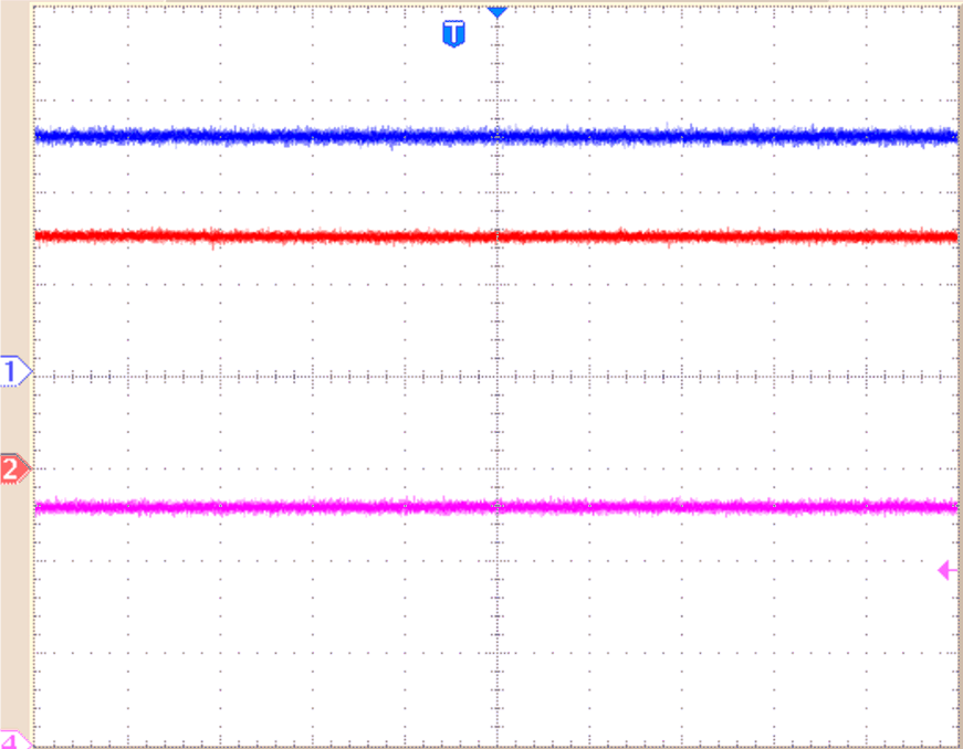
Figure 25 shows a typical topology used to introduce additional hysteresis. The additional hysteresis depends on the external resistors value and the supply voltage VDD.
Table 2. Design Parameters
| PARAMETER | VALUE |
|---|---|
| Supply voltage | 5 V |
| VIN | 2.5 V and 50 mV noise on top |
| Ceramic capacitor | XR5 or XR7 50V |
| Hysteresis V+(H) – V+(-) | 70 mV |
| R1, R2 | 27K 1% |
| R | 1MΩ 1% |
9.2.1.2 Detailed Design Procedure
This circuit is designed for stabilizing the output in a noisy environment by adding external hysteresis. The hysteresis is added by connecting a feedback resistor between positive input V+ and output VOUT. Output is high and VOUT = VDD, the positive input V+(H) =

Output is low and VOUT = GND, the positive input V+(L) =

From Equation 1 and Equation 2:


9.2.2 Two-Phase Non-Overlapping Clock Generator
9.2.2.1 Design Requirements
Table 3 lists the design parameters.
Table 3. Design Parameters
| PARAMETER | VALUE |
|---|---|
| Supply voltage | 3 V to 12 V |
| Ceramic capacitor | XR5 or XR7 50 V |
| Resistors | 1% |
9.2.2.2 Detailed Design Procedure
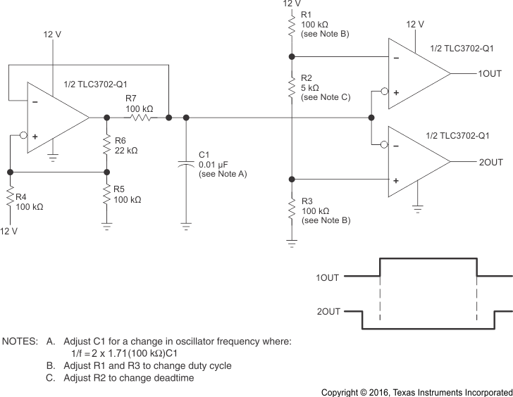
The first stage is a window comparator with positive feedback by connecting R6 between the comparator output and the positive input. That creates an external hysteresis depending on resistors R4, R5, R6 value and the supply voltage VDD.
Comparator output is high gives V+(H) =

Comparator output is low gives V+(L) =

The negative feedback between capacitor C1 and the comparator negative input allows the capacitor to charge between 2 threshold V+(H) and V+(L). The charging and discharging is exponential with time constant of R7C1. The charging and discharging have the same duration.
C1 is charging during the time when output is high and the voltage across it is:

The charging time is:

The charging and discharging time is:

and the oscillator frequency is:

For the circuit of Figure 28, V+(L) = 1.83 V, V+(H) = 10.17 V and period T = 3.43 mS
This circuit can also be used for Frequency Dithering in switch mode power supply to pass EMC compliance.
The second stage forms 2 window comparators with complementary outputs. One output 1OUT is high when

VDD and 2OUT is high when


