SLVS695D June 2007 – January 2015 TLC5916 , TLC5917
PRODUCTION DATA.
- 1 Features
- 2 Applications
- 3 Description
- 4 Revision History
- 5 Device Comparison Table
- 6 Pin Configuration and Functions
-
7 Specifications
- 7.1 Absolute Maximum Ratings
- 7.2 ESD Ratings
- 7.3 Recommended Operating Conditions
- 7.4 Thermal Information
- 7.5 Electrical Characteristics: VDD = 3 V
- 7.6 Electrical Characteristics: VDD = 5.5 V
- 7.7 Switching Characteristics: VDD = 3 V
- 7.8 Switching Characteristics: VDD = 5.5 V
- 7.9 Timing Requirements
- 7.10 Typical Characteristics
- 8 Parameter Measurement Information
- 9 Detailed Description
- 10Application and Implementation
- 11Power Supply Recommendations
- 12Layout
- 13Device and Documentation Support
- 14Mechanical, Packaging, and Orderable Information
Package Options
Mechanical Data (Package|Pins)
Thermal pad, mechanical data (Package|Pins)
Orderable Information
10 Application and Implementation
NOTE
Information in the following applications sections is not part of the TI component specification, and TI does not warrant its accuracy or completeness. TI’s customers are responsible for determining suitability of components for their purposes. Customers should validate and test their design implementation to confirm system functionality.
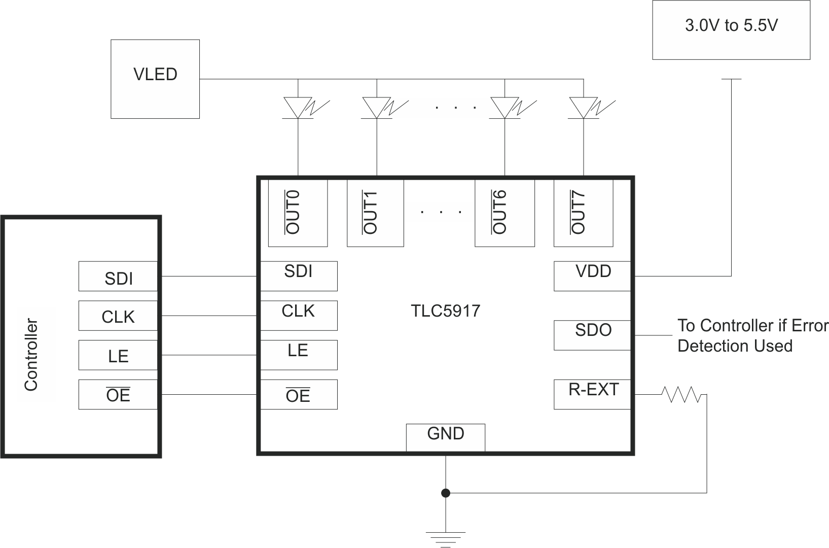
10.1 Application Information
10.1.1 Constant Current
In LED display applications, TLC591x provides nearly no current variations from channel to channel and from IC to IC. While 5 mA ≤ IOUT ≤ 100 mA, the maximum current skew between channels is less than ±3% and between ICs is less than ±6%.
10.1.2 Adjusting Output Current
TLC591x scales up the reference current, Iref, set by the external resistor Rext to sink a current, Iout, at each output port. Users can follow the below formulas to calculate the target output current IOUT,target in the saturation region. In the equations,
Rext is the resistance of the external resistor connected between the R-EXT terminal and ground and VR-EXT is the voltage of R-EXT, which is controlled by the programmable voltage gain (VG). VG is defined by the Configuration Code.
The Current Multiplier (CM) determines that the ratio IOUT,target/Iref is 15 or 5. After power on, the default value of VG is 127/128 = 0.992, and the default value of CM is 1, so that the ratio IOUT,target/Iref = 15. Based on the default VG and CM:
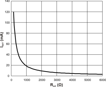
Therefore, the default current is approximately 52 mA at 360 Ω and 26 mA at 720 Ω. The default relationship after power on between IOUT,target and Rext is shown in Figure 19.
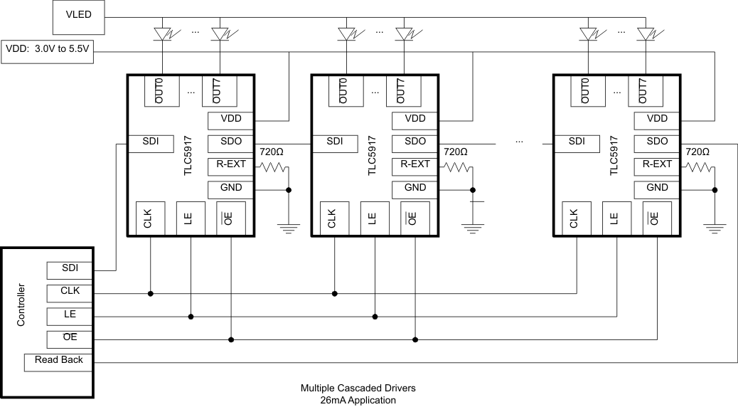
10.1.3 Cascading Implementation of TLC591x Device
10.1.4 8-Bit Configuration Code and Current Gain
Bit definition of the Configuration Code in the Configuration Latch is shown in Table 5.
Table 5. Bit Definition of 8-Bit Configuration Code
| 0 | 1 | 2 | 3 | 4 | 5 | 6 | 7 | |
|---|---|---|---|---|---|---|---|---|
| Meaning | CM | HC | CC0 | CC1 | CC2 | CC3 | CC4 | CC5 |
| Default | 1 | 1 | 1 | 1 | 1 | 1 | 1 | 1 |
Bit 7 is first sent into TLC591x through SDI. Bits 1 to 7 {HC, CC[0:5]} determine the voltage gain (VG) that affects the voltage at R-EXT and indirectly affects the reference current, Iref, flowing through the external resistor at R-EXT. Bit 0 is the Current Multiplier (CM) that determines the ratio IOUT,target/Iref. Each combination of VG and CM gives a specific Current Gain (CG).
- VG: the relationship between {HC,CC[0:5]} and the voltage gain is calculated as shown in Equation 6 and Equation 7:
- CM: In addition to determining the ratio IOUT,target/Iref, CM limits the output current range.
- CG: The total Current Gain is defined as the following.
Where HC is 1 or 0, and D is the binary value of CC[0:5]. So, the VG could be regarded as a floating-point number with 1-bit exponent HC and 6-bit mantissa CC[0:5]. {HC,CC[0:5]} divides the programmable voltage gain VG into 128 steps and two sub-bands:
Low voltage sub-band (HC = 0): VG = 1/4 ~ 127/256, linearly divided into 64 steps
High voltage sub-band (HC = 1): VG = 1/2 ~ 127/128, linearly divided into 64 steps
High Current Multiplier (CM = 1): IOUT,target/Iref = 15, suitable for output current range IOUT = 10 mA to 120 mA.
Low Current Multiplier (CM = 0): IOUT,target/Iref = 5, suitable for output current range IOUT = 3 mA to 40 mA
Therefore, CG = (1/12) to (127/128), and it is divided into 256 steps. If CG = 127/128 = 0.992, the IOUT,target-Rext.
Examples
- Configuration Code {CM, HC, CC[0:5]} = {1,1,111111}
- Configuration Code = {1,1,000000}
- Configuration Code = {0,0,000000}
VG = 127/128 = 0.992 and CG = VG × 30 = VG = 0.992
VG = (1 + 1) × (1 + 0/64)/4 = 1/2 = 0.5, and CG = 0.5
VG = (1 + 0) × (1 + 0/64)/4 = 1/4, and CG = (1/4) × 3–1 = 1/12
After power on, the default value of the Configuration Code {CM, HC, CC[0:5]} is {1,1,111111}. Therefore, VG = CG = 0.992. The relationship between the Configuration Code and the Current Gain is shown in Figure 21.
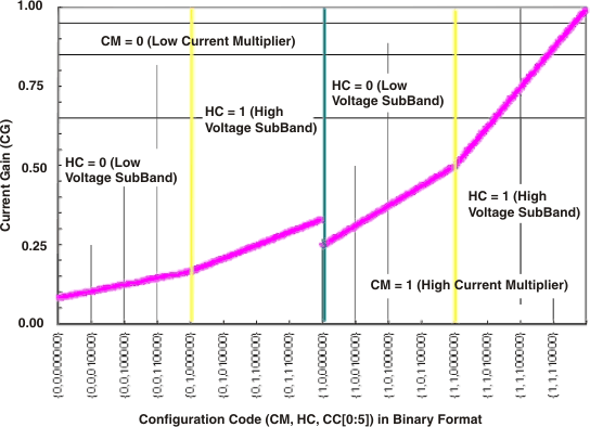 Figure 21. Current Gain vs Configuration Code
10.2 Typical Application
Figure 22 shows implementation of a single TLC591x device. Figure 20 shows a cascaded driver implementation.
10.2.1 Design Requirements
For this design example, use the parameters listed in Table 6. The purpose of this design procedure is to calculate the power dissipation in the device and the operating junction temperature.
Table 6. Design Parameters
| DESIGN PARAMETERS | EXAMPLE VALUE |
|---|---|
| Number of LED strings | 8 |
| Number of LEDs per string | 3 |
| LED Current (mA) | 20 |
| Forward voltage of each LED (V) | 3.5 |
| Junction-to-ambient thermal resistance (°C/W) | 87.4 |
| Ambient temperature of application (°C) | 115 |
| VDD (V) | 5 |
| IDD (mA) | 10 |
| Max operating junction temperature (°C) | 150 |
10.2.2 Detailed Design Procedure
where
- TJ is the junction temperature.
- TA is the ambient temperature.
- RθJA is the junction-to-ambient thermal resistance.
- PD_TOT is the total power dissipation in the IC.
where
- PD_CSis the power dissipation in the LED current sinks.
- IDD is the IC supply current.
- VDD is the IC supply voltage.
where
- IO is the LED current.
- VO is the voltage at the output pin.
- nCH is the number of LED strings.
where
- VLED is the voltage applied to the LED string.
- nLED is the number of LEDs in the string.
- VF is the forward voltage of each LED.
VO must not be too high as this causes excess power dissipation inside the current sink. However, VO also must not be too low as this does not allow the full LED current (Figure 4). With VLED = 12 V:
Using PD_CS, calculate:
Using PD_TOT, calculate:
This design example demonstrates how to calculate power dissipation in the IC and ensure that the junction temperature is kept below 150°C.
NOTE
This design example assumes that all channels have the same electrical parameters (nLED, IO, VF, VLED). If the parameters are unique for each channel, then the power dissipation must be calculated for each current sink separately. Then, each result must be added together to calculate the total power dissipation in the current sinks.
10.2.3 Application Curve
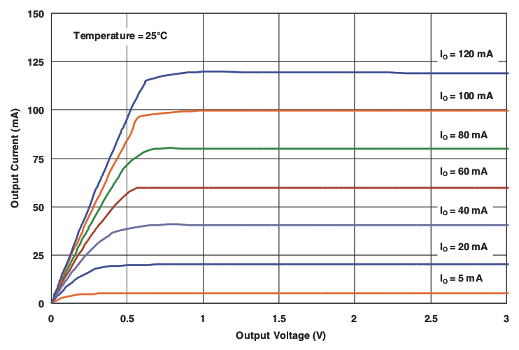 Figure 23. Output Current vs Output Voltage