SLVS695D June 2007 – January 2015 TLC5916 , TLC5917
PRODUCTION DATA.
- 1 Features
- 2 Applications
- 3 Description
- 4 Revision History
- 5 Device Comparison Table
- 6 Pin Configuration and Functions
-
7 Specifications
- 7.1 Absolute Maximum Ratings
- 7.2 ESD Ratings
- 7.3 Recommended Operating Conditions
- 7.4 Thermal Information
- 7.5 Electrical Characteristics: VDD = 3 V
- 7.6 Electrical Characteristics: VDD = 5.5 V
- 7.7 Switching Characteristics: VDD = 3 V
- 7.8 Switching Characteristics: VDD = 5.5 V
- 7.9 Timing Requirements
- 7.10 Typical Characteristics
- 8 Parameter Measurement Information
- 9 Detailed Description
- 10Application and Implementation
- 11Power Supply Recommendations
- 12Layout
- 13Device and Documentation Support
- 14Mechanical, Packaging, and Orderable Information
Package Options
Mechanical Data (Package|Pins)
Thermal pad, mechanical data (Package|Pins)
Orderable Information
9 Detailed Description
9.1 Overview
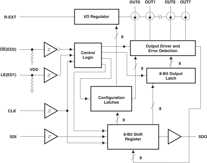
The TLC591x is designed for LED displays and LED lighting applications with constant-current control and open-load, shorted-load, and overtemperature detection. The TLC591x contains an 8-bit shift register and data latches, which convert serial input data into parallel output format. At the output stage, eight regulated current ports are designed to provide uniform and constant current for driving LEDs within a wide range of LED Forward Voltage (VF) variations. Used in system design for LED display applications, for example, LED panels, it provides great flexibility and device performance. Users can adjust the output current from 3 mA to 120 mA per channel through an external resistor, Rext, which gives flexibility in controlling the light intensity of LEDs. The devices are designed for up to 20 V at the output port. The high clock frequency, 30 MHz, also satisfies the system requirements of high-volume data transmission.
The TLC591x provides two operation modes: Normal Mode and Special Mode. Normal mode is used for shifting LED data into and out of the driver. Special Mode includes two functions: Error Detection and Current Gain Control. The two operation modes include three phases: Normal Mode phase, Mode Switching transition phase, and Special Mode phase. The signal on the multiple function pin OE(ED2) is monitored to determine the mode. When a one-clock-wide pulse appears on OE(ED2), the device enters the Mode Switching phase. At this time, the voltage level on LE(ED1) determines which mode the TLC591x switches to.
In the Normal Mode phase, the serial data can be transferred into TLC591x through the pin SDI, shifted in the shift register, and transferred out via the pin SDO. LE(ED1) can latch the serial data in the shift register to the output latch. OE(ED2) enables the output drivers to sink current.
In the Special Mode phase, the low-voltage-level signal on OE(ED2) can enable output channels and detect the status of the output current to determine if the driving current level is sufficient. The detected Error Status is loaded into the 8-bit shift register and shifted out via the pin SDO, synchronous to the CLK signal. The system controller can read the error status and determine if the LEDs are properly lit.
In the Special Mode phase, the TLC591x allows users to adjust the output current level by setting a runtime-programmable Configuration Code. The code is sent into the TLC591x through SDI. The positive pulse of LE(ED1) latches the code in the shift register into a built-in 8-bit configuration latch, instead of the output latch. The code affects the voltage at the terminal R-EXT and controls the output-current regulator. The output current can be finely adjusted by a gain ranging from 1/12 to 127/128 in 256 steps. Therefore, the current skew between ICs can be compensated within less than 1%. This feature is suitable for white balancing in LED color display panels.
9.2 Functional Block Diagram
9.3 Feature Description
9.3.1 Open-Circuit Detection Principle
The LED Open-Circuit Detection compares the effective current level Iout with the open load detection threshold current IOUT,Th. If IOUT is below the IOUT,Th threshold, the TLC591x detects an open-load condition. This error status can be read as an error status code in the Special Mode. For open-circuit error detection, a channel must be on.
9.3.2 Short-Circuit Detection Principle (TLC5917 Only)
The LED short-circuit detection compares the effective voltage level (VOUT) with the shorted-load detection threshold voltages VOUT,TTh and VOUT,RTh. If VOUT is above the VOUT,TTh threshold, the TLC5917 detects an shorted-load condition. If VOUT is below the VOUT,RTh threshold, no error is detected/error bit is reset. This error status can be read as an error status code in the Special Mode. For short-circuit error detection, a channel must be on.
Table 2. Shorted-Load Detection
| STATE OF OUTPUT PORT | CONDITION OF OUTPUT VOLTAGE | ERROR STATUS CODE | MEANING |
|---|---|---|---|
| Off | IOUT = 0 mA | 0 | Detection not possible |
| On | VOUT ≥ VOUT,TTh | 0 | Short circuit |
| VOUT < VOUT,RTh | 1 | Normal |
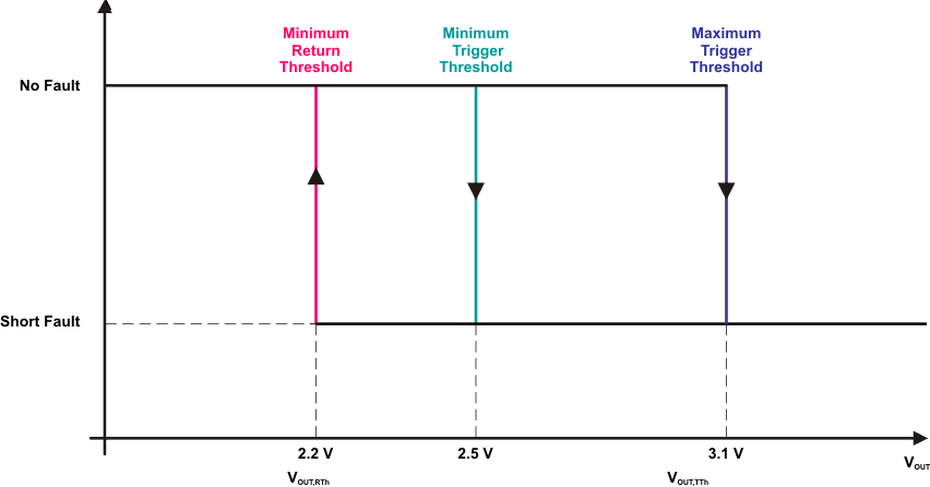 Figure 10. Short-Circuit Detection Principle
9.3.3 Overtemperature Detection and Shutdown
TLC591x is equipped with a global overtemperature sensor and eight individual, channel-specific, overtemperature sensors.
- When the global sensor reaches the trip temperature, all output channels are shut down, and the error status is stored in the internal Error Status register of every channel. After shutdown, the channels automatically restart after cooling down, if the control signal (output latch) remains on. The stored error status is not reset after cooling down and can be read out as the error status code in the Special Mode.
- When one of the channel-specific sensors reaches trip temperature, only the affected output channel is shut down, and the error status is stored only in the internal Error Status register of the affected channel. After shutdown, the channel automatically restarts after cooling down, if the control signal (output latch) remains on. The stored error status is not reset after cooling down and can be read out as error status code in the Special Mode.
For channel-specific overtemperature error detection, a channel must be on.
The error status code is reset when TLC591x returns to Normal Mode.
Table 3. Overtemperature Detection(1)
| STATE OF OUTPUT PORT | CONDITION | ERROR STATUS CODE | MEANING |
|---|---|---|---|
| Off | IOUT = 0 mA | 0 | |
| On On → all channels Off |
Tj < Tj,trip global | 1 | Normal |
| Tj > Tj,trip global | All error status bits = 0 | Global overtemperature | |
| On On → Off |
Tj < Tj,trip channel n | 1 | Normal |
| Tj > Tj,trip channel n | Channel n error status bit = 0 | Channel n overtemperature |
9.4 Device Functional Modes
The TLC591x provides two operation modes: Normal Mode and Special Mode. Normal mode is used for shifting LED data into and out of the driver. Special Mode includes two functions: Error Detection and Current Gain Control. The two operation modes include three phases: Normal Mode phase, Mode Switching transition phase, and Special Mode phase. The signal on the multiple function pin OE(ED2) is monitored to determine the mode. When a one-clock-wide pulse appears on OE(ED2), the device enters the Mode Switching phase. At this time, the voltage level on LE(ED1) determines which mode the TLC591x switches to.
In the Normal Mode phase, the serial data can be transferred into TLC591x through the pin SDI, shifted in the shift register, and transferred out via the pin SDO. LE(ED1) can latch the serial data in the shift register to the output latch. OE(ED2) enables the output drivers to sink current.
In the Special Mode phase, the low-voltage-level signal on OE(ED2) can enable output channels and detect the status of the output current to determine if the driving current level is sufficient. The detected Error Status is loaded into the 8-bit shift register and shifted out via the pin SDO, synchronous to the CLK signal. The system controller can read the error status and determine if the LEDs are properly lit.
In the Special Mode phase, the TLC591x allows users to adjust the output current level by setting a runtime-programmable Configuration Code. The code is sent into the TLC591x through SDI. The positive pulse of LE(ED1) latches the code in the shift register into a built-in 8-bit configuration latch, instead of the output latch. The code affects the voltage at the terminal R-EXT and controls the output-current regulator. The output current can be finely adjusted by a gain ranging from 1/12 to 127/128 in 256 steps. Therefore, the current skew between ICs can be compensated within less than 1%. This feature is suitable for white balancing in LED color display panels.
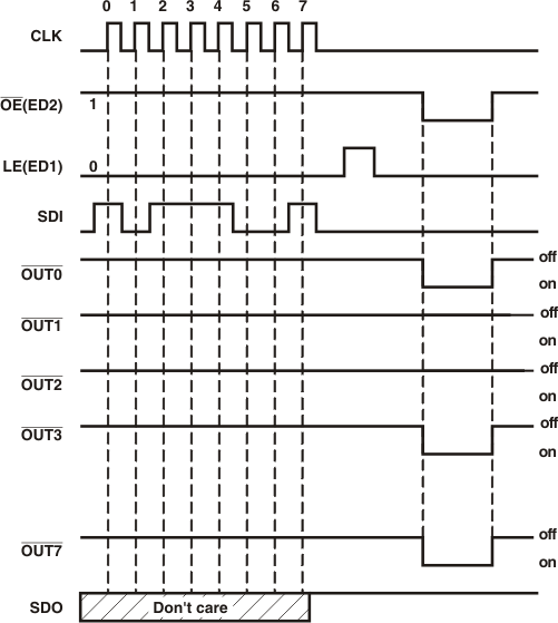 Figure 11. Normal Mode
Table 4. Truth Table in Normal Mode
| CLK | LE(ED1) | OE(ED2) | SDI | OUT0...OUT7 | SDO |
|---|---|---|---|---|---|
| ↑ | H | L | Dn | Dn...Dn – 7 | Dn – 7 |
| ↑ | L | L | Dn + 1 | No change | Dn – 6 |
| ↑ | H | L | Dn + 2 | Dn + 2...Dn – 5 | Dn – 5 |
| ↓ | X | L | Dn + 3 | Dn + 2...Dn – 5 | Dn – 5 |
| ↓ | X | H | Dn + 3 | Off | Dn – 5 |
The signal sequence shown in Figure 12 makes the TLC591x enter Current Adjust and Error Detection Mode.
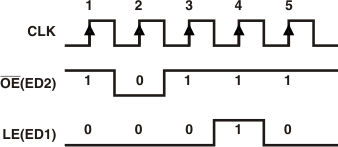 Figure 12. Switching to Special Mode
In the Current Adjust Mode, sending the positive pulse of LE(ED1), the content of the shift register (a current adjust code) is written to the 8-bit configuration latch (see Figure 13).
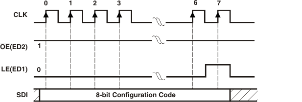 Figure 13. Writing Configuration Code
When the TLC591x is in the Error Detection Mode, the signal sequence shown in Figure 14 enables a system controller to read error status codes through SDO.
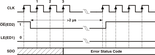 Figure 14. Reading Error Status Code
The signal sequence shown in Figure 15 makes TLC591x resume the Normal Mode. Switching to Normal Mode resets all internal Error Status registers. OE(ED2) always enables the output port, whether the TLC591x enters Current Adjust Mode or not.
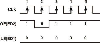 Figure 15. Switching to Normal Mode
9.4.1 Operation Mode Switching
To switch between its two modes, TLC591x monitors the signal OE(ED2). When an one-clock-wide pulse of OE(ED2) appears, TLC591x enters the two-clock-period transition phase, the Mode Switching phase. After power on, the default operation mode is the Normal Mode (see Figure 16).
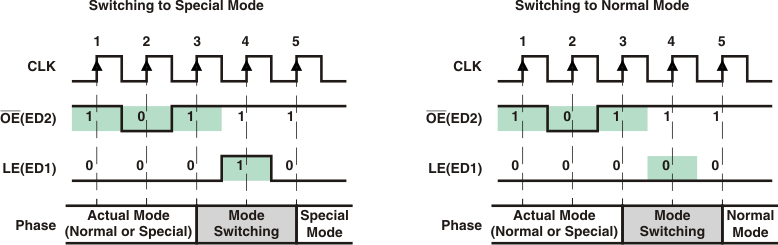 Figure 16. Mode Switching
As shown in Figure 16, once a one-clock-wide short pulse (101) of OE(ED2) appears, TLC591x enters the Mode Switching phase. At the fourth rising edge of CLK, if LE(ED1) is sampled as voltage high, TLC591x switches to Special Mode; otherwise, it switches to Normal Mode. The signal LE(ED1) between the third and the fifth rising edges of CLK cannot latch any data. Its level is used only to determine into which mode to switch. However, the short pulse of OE(ED2) can still enable the output ports. During mode switching, the serial data can still be transferred through SDI and shifted out from SDO.
NOTE
- The signal sequence for the mode switching may be used frequently to ensure that TLC591x is in the proper mode.
- The 1 and 0 on the LE(ED1) signal are sampled at the rising edge of CLK. The X means its level does not affect the result of mode switching mechanism.
- After power on, the default operation mode is Normal Mode.
9.4.1.1 Normal Mode Phase
Serial data is transferred into TLC591x through SDI, shifted in the Shift Register, and output via SDO. LE(ED1) can latch the serial data in the Shift Register to the Output Latch. OE(ED2) enables the output drivers to sink current. These functions differ only as described in Operation Mode Switching, in which case, a short pulse triggers TLC591x to switch the operation mode. However, as long as LE(ED1) is high in the Mode Switching phase, TLC591x remains in the Normal Mode, as if no mode switching occurred.
9.4.1.2 Special Mode Phase
In the Special Mode, as long as OE(ED2) is not low, the serial data is shifted to the Shift Register via SDI and shifted out via SDO, as in the Normal Mode. However, there are two differences between the Special Mode and the Normal Mode, as shown in the following sections.
9.4.2 Reading Error Status Code in Special Mode
When OE(ED2) is pulled low while in Special Mode, error detection and load error status codes are loaded into the Shift Register, in addition to enabling output ports to sink current. Figure 17 shows the timing sequence for error detection. The 0 and 1 signal levels are sampled at the rising edge of each CLK. At least three zeros must be sampled at the voltage low signal OE(ED2). Immediately after the second zero is sampled, the data input source of the Shift Register changes to the 8-bit parallel Error Status Code register, instead of from the serial data on SDI. Normally, the error status codes are generated at least 2 μs after the falling edge of OE(ED2). The occurrence of the third or later zero saves the detected error status codes into the Shift Register. Therefore, when OE(ED2) is low, the serial data cannot be shifted into TLC591x through SDI. When OE(ED2) is pulled high, the data input source of the Shift Register is changed back to SDI. At the same time, the output ports are disabled and the error detection is completed. Then, the error status codes saved in the Shift Register can be shifted out via SDO bit by bit along with CLK, as well as the new serial data can be shifted into TLC591x through SDI.
While in Special Mode, the TLC591x cannot simultaneously transfer serial data and detect LED load error status.
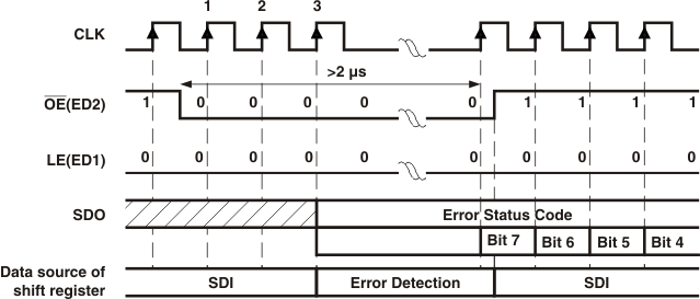 Figure 17. Reading Error Status Code
9.4.3 Writing Configuration Code in Special Mode
When in Special Mode, the active high signal LE(ED1) latches the serial data in the Shift Register to the Configuration Latch, instead of the Output Latch. The latched serial data is used as the Configuration Code.
The code is stored until power off or the Configuration Latch is rewritten. As shown in Figure 18, the timing for writing the Configuration Code is the same as the timing in the Normal Mode to latching output channel data. Both the Configuration Code and Error Status Code are transferred in the common 8-bit Shift Register. Users must pay attention to the sequence of error detection and current adjustment to avoid the Configuration Code being overwritten by Error Status Code.
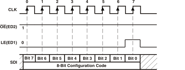 Figure 18. Writing Configuration Code