SBVS114B July 2008 – January 2015 TLC5947
PRODUCTION DATA.
- 1 Features
- 2 Applications
- 3 Description
- 4 Revision History
- 5 Pin Configuration and Functions
- 6 Specifications
- 7 Parameter Measurement Information
- 8 Detailed Description
- 9 Application and Implementation
- 10Power Supply Recommendations
- 11Layout
- 12Device and Documentation Support
- 13Mechanical, Packaging, and Orderable Information
Package Options
Mechanical Data (Package|Pins)
Thermal pad, mechanical data (Package|Pins)
Orderable Information
9 Application and Implementation
NOTE
Information in the following applications sections is not part of the TI component specification, and TI does not warrant its accuracy or completeness. TI’s customers are responsible for determining suitability of components for their purposes. Customers should validate and test their design implementation to confirm system functionality.
9.1 Application Information
The device is a 24-channel, constant sink current, LED driver. This device can be connected in series to drive many LED lamps with only a few controller ports. Output current control data and PWM control data can be written from the SIN input terminal. The PWM timing reference clock can be supplied from the internal oscillation.
9.2 Typical Application
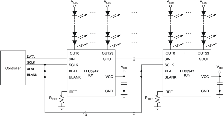 Figure 23. Typical Application Circuit (Multiple Daisy Chained TLC5947s)
9.2.1 Design Requirements
For this design example, use Table 2 as the input parameters.
Table 2. Design Parameters
| DESIGN PARAMETER | EXAMPLE VALUE |
|---|---|
| VCC input voltage range | 3 V to 5.5 V |
| LED lamp (VLED) input voltage range | Maximum LED forward voltage (VF) + IC knee voltage |
| SIN, SCLK, LAT, and BLANK voltage range | Low level = GND, High level = VCC |
9.2.2 Detailed Design Procedure
9.2.2.1 Define Basic Parameters
To begin the design process, a few parameters must be decided as following:
- Maximum output constant-current value for each color LED lamp
- Maximum LED forward voltage (VF)
- Are auto display function used
9.2.2.2 Grayscale (GS) Data
There are a total of 24 sets of 12-bit GS data for the PWM control of each output. Select the GS data of each LED lamp and write the GS data to the register following the signal timing.
9.2.2.3 Auto-Display Function
There are a total of 24 sets of 12-bit GS data for the PWM control of each output. Select the GS data of each LED lamp and write the GS data to the register following the signal timing.
9.2.2.4 Setting for the Constant Sink Current Value
The constant-current value for all channels is set by an external resistor (RIREF) placed between IREF and GND. The resistor (RIREF) value is calculated by Equation 2.
where
- VIREF = the internal reference voltage on the IREF pin (typically 1.20 V).
IOLC must be set in the range of 2 mA to 30 mA. The constant sink current characteristic for the external resistor value is shown in Figure 4. Table 3 describes the constant-current output versus external resistor value.
Table 3. Constant-Current Output versus External Resistor Value
| IOLC (mA, Typical) | RIREF (Ω) |
|---|---|
| 30 | 1640 |
| 25 | 1968 |
| 20 | 2460 |
| 15 | 3280 |
| 10 | 4920 |
| 5 | 9840 |
| 2 | 24600 |
9.2.3 Application Curves
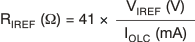
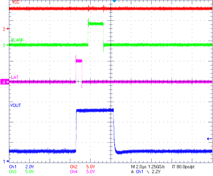 Figure 24. Output Waveform with GS Data Latch Input
 Figure 25. Output Waveform without GS Data Latch Input