SBVS114B July 2008 – January 2015 TLC5947
PRODUCTION DATA.
- 1 Features
- 2 Applications
- 3 Description
- 4 Revision History
- 5 Pin Configuration and Functions
- 6 Specifications
- 7 Parameter Measurement Information
- 8 Detailed Description
- 9 Application and Implementation
- 10Power Supply Recommendations
- 11Layout
- 12Device and Documentation Support
- 13Mechanical, Packaging, and Orderable Information
Package Options
Mechanical Data (Package|Pins)
Thermal pad, mechanical data (Package|Pins)
Orderable Information
11 Layout
11.1 Layout Guidelines
- Place the decoupling capacitor near the VCC pin and GND plane.
- Place the current programming resistor RIREF close to the IREF pin and the IREFGND pin.
- Route the GND pattern as widely as possible for large GND currents.
- The routing wire between the LED cathode side and the device OUTXn pin must be as short and straight as possible to reduce wire inductance.
- When several ICs are chained, symmetric placements are recommended.
11.2 Layout Example
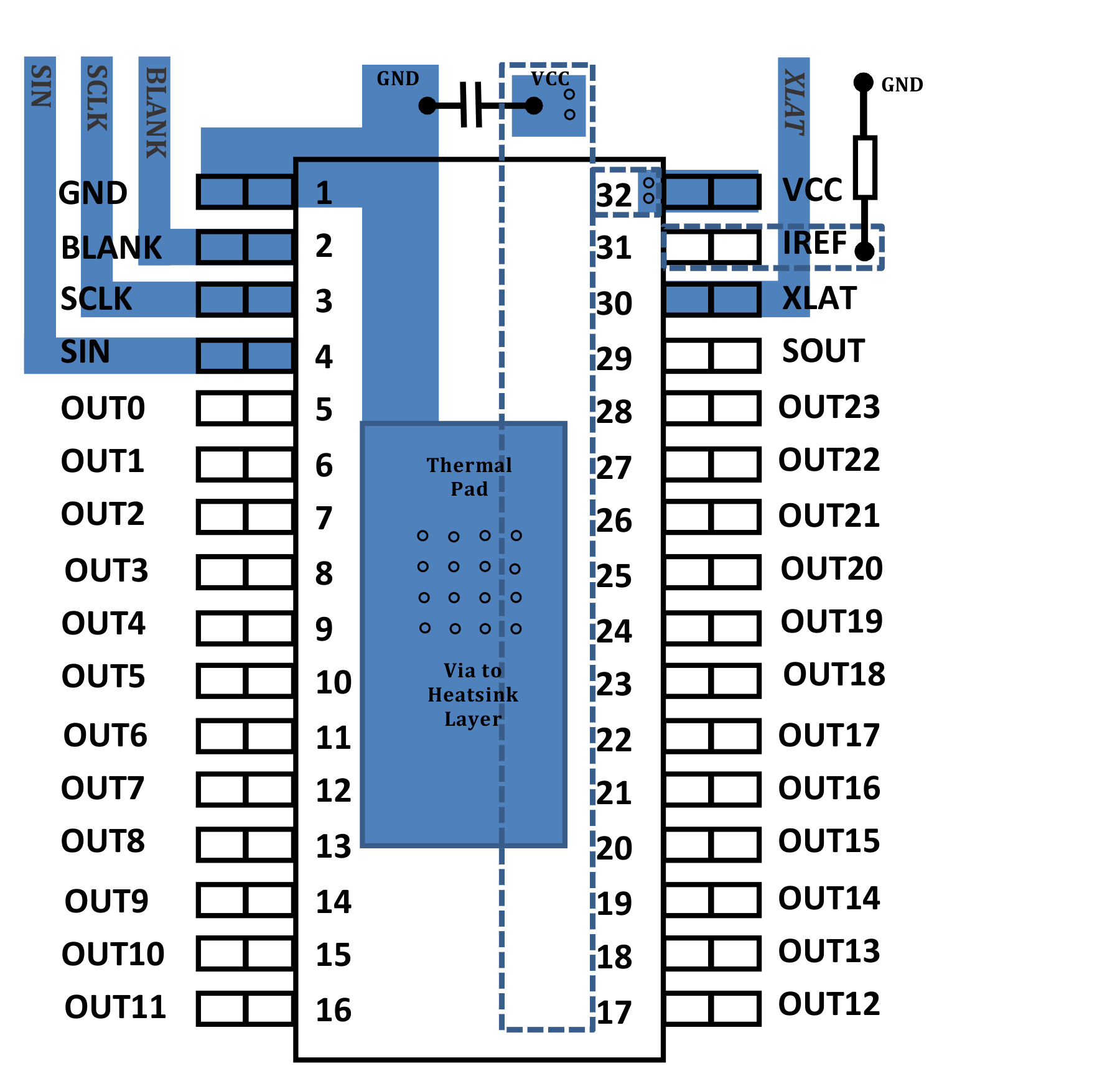 Figure 26. Layout Schematic
11.3 Power Dissipation
The device power dissipation must be below the power dissipation rate of the device package (illustrated in Figure 5) to ensure correct operation. Equation 4 calculates the power dissipation of the device:
Equation 4. 
where
- VCC = device supply voltage
- ICC = device supply current
- VOUT = OUTn voltage when driving LED current
- IOLC = LED current adjusted by RIREF resistor
- N = number of OUTn driving LED at the same time
- dPWM = duty ratio defined by GS value