SLVSCQ4 October 2014 TLC5957
PRODUCTION DATA.
- 1 Features
- 2 Applications
- 3 Description
- 4 Typical Application Circuit (Multiple Daisy Chained TLC5957s)
- 5 Revision History
- 6 Pin Configuration and Functions
- 7 Specifications
- 8 Parameter Measurement Information
-
9 Detailed Description
- 9.1 Overview
- 9.2 Functional Block Diagram
- 9.3
Device Functional Modes
- 9.3.1 Brightness Control (BC) Function
- 9.3.2 Color Control (CC) Function
- 9.3.3 Select RIREF For a Given BC
- 9.3.4 Choosing BC/CC For a Different Application
- 9.3.5 LED Open Detection (LOD)
- 9.3.6 Poker Mode
- 9.3.7 Internal Circuit for Caterpillar Removal
- 9.3.8 Internal Pre-charge FET for Ghost Removal
- 9.3.9 Thermal Shutdown (TSD)
- 9.3.10 IREF Resistor Short Protection (ISP)
- 9.3.11 Noise Reduction
- 10Application and Implementation
- 11Power Supply Recommendations
- 12Layout
- 13Device and Documentation Support
- 14Mechanical, Packaging, and Orderable Information
Package Options
Mechanical Data (Package|Pins)
- RTQ|56
Thermal pad, mechanical data (Package|Pins)
- RTQ|56
Orderable Information
6 Pin Configuration and Functions
RTQ
56 PINS
Top View
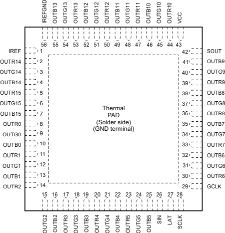
Pin Functions
| PIN | I/O | DESCRIPTION | |
|---|---|---|---|
| NAME | NO. | ||
| GCLK | 29 | I | Grayscale(GS) pulse width modulation (PWM) reference clock control for OUTXn. |
| Each GCLK rising edge increase the GS counter by1 for PWM control. | |||
| GND | ThermalPad | — | Power ground. The thermal pad must be soldered to GND on PCB. |
| IREF | 1 | — | Maximum constant-current value setting. The OUTR0 to OUTB15 maximum constant output current are set to the desired values by connecting an external resistor between IREF and IREFGND. See Equation 1 for more detail. The external resistor should be placed close to the device. |
| IREFGND | 56 | — | Analog ground. Dedicated ground pin for the external IREF resistor. This pin should be connected to analog ground trace which is connected to power ground near the common GND point of board. |
| LAT | 27 | I | The LAT falling edge latches the data from the common shift register into the GS data latch or FC data latch. |
| OUTR0-R15 | 8, 11, 14, 17, 20, 23, 30, 33, 36, 39, 44, 47, 50, 53, 2, 5 | O | Constant current output for RED LED. Multiple outputs can be tied together to increase the constant current capability. Different voltages can be applied to each output. These outputs are turned on-off by GCLK signal and the data in GS data memory. |
| OUTG0-G15 | 9, 12, 15, 18, 21, 24, 31, 34, 37, 40, 45, 48, 51, 54, 3, 6 | O | Constant current output for GREEN LED. Multiple outputs can be tied together to increase the constant current capability. Different voltages can be applied to each output. These outputs are turned on-off by GCLK signal and the data in GS data memory. |
| OUTB0-B15 | 10, 13, 16, 19, 22, 25, 32, 35, 38, 41, 46, 49, 52, 55, 4, 7 | O | Constant current output for BLUE LED. Multiple outputs can be tied together to increase the constant current capability. Different voltages can be applied to each output. These outputs are turned on-off by GCLK signal and the data in GS data memory. |
| SCLK | 28 | I | Serial data shift clock. Data present on SIN are shifted to the 48-bit common shift register LSB with the SCLK rising edge. Data in the shift register are shifted towards the MSB at each SCLK rising edge. The common shift register MSB appears on SOUT. |
| SIN | 26 | I | Serial data input of the 48-bit common shift register. When SIN is high level, the LSB is set to '1' for only one SCLK input rising edge. If two SCLK rising edges are input while SIN is high, then the 48-bit shift register LSB and LSB+1 are set to '1'. When SIN is low, the LSB is set to '0' at the SCLK input rising edge. |
| SOUT | 42 | O | Serial data output of the 48-bit common shift register. SOUT is connected to the MSB of the register. |
| VCC | 43 | — | Power-supply voltage. |