SLVSCQ4 October 2014 TLC5957
PRODUCTION DATA.
- 1 Features
- 2 Applications
- 3 Description
- 4 Typical Application Circuit (Multiple Daisy Chained TLC5957s)
- 5 Revision History
- 6 Pin Configuration and Functions
- 7 Specifications
- 8 Parameter Measurement Information
-
9 Detailed Description
- 9.1 Overview
- 9.2 Functional Block Diagram
- 9.3
Device Functional Modes
- 9.3.1 Brightness Control (BC) Function
- 9.3.2 Color Control (CC) Function
- 9.3.3 Select RIREF For a Given BC
- 9.3.4 Choosing BC/CC For a Different Application
- 9.3.5 LED Open Detection (LOD)
- 9.3.6 Poker Mode
- 9.3.7 Internal Circuit for Caterpillar Removal
- 9.3.8 Internal Pre-charge FET for Ghost Removal
- 9.3.9 Thermal Shutdown (TSD)
- 9.3.10 IREF Resistor Short Protection (ISP)
- 9.3.11 Noise Reduction
- 10Application and Implementation
- 11Power Supply Recommendations
- 12Layout
- 13Device and Documentation Support
- 14Mechanical, Packaging, and Orderable Information
Package Options
Mechanical Data (Package|Pins)
- RTQ|56
Thermal pad, mechanical data (Package|Pins)
- RTQ|56
Orderable Information
7 Specifications
7.1 Absolute Maximum Ratings
over operating free-air temperature range (unless otherwise noted) (1)| MIN | MAX | UNIT | |||
|---|---|---|---|---|---|
| VCC(2) | Supply voltage | VCC | –0.3 | 6.0 | V |
| IOUT | Output current (dc) | OUTx0 to OUTx15, x = R, G, B | 30 | 30 | mA |
| VIN(2) | Input voltage range | SIN, SCLK, LAT, GCLK, IREF | –0.3 | VCC + 0.3 | V |
| VOUT(2) | Output voltage range | SOUT | –0.3 | VCC + 0.3 | V |
| OUTx0 to OUTx15, x = R, G, B | –0.3 | 11 | V | ||
| TJ(MAX) | Operation junction temperature | –40 | 150 | °C | |
(1) Stresses beyond those listed under Absolute Maximum Ratings may cause permanent damage to the device. These are stress ratings only, which do not imply functional operation of the device at these or any other conditions beyond those indicated under Recommended Operating Conditions. Exposure to absolute-maximum-rated conditions for extended periods may affect device reliability.
(2) All voltage values are with respect to device ground terminal.
7.2 Handling Ratings
| MIN | MAX | UNIT | |||
|---|---|---|---|---|---|
| Tstg | Storage temperature range | –55 | 150 | °C | |
| V(ESD) | Electrostatic discharge | Human body model (HBM), per ANSI/ESDA/JEDEC JS-001, all pins(1) | –3 | 3 | kV |
| Charged device model (CDM), per JEDEC specification JESD22-C101, all pins(2) | –1 | 1 | |||
(1) JEDEC document JEP155 states that 500-V HBM allows safe manufacturing with a standard ESD control process.
(2) JEDEC document JEP157 states that 250-V CDM allows safe manufacturing with a standard ESD control process.
7.3 Recommended Operating Conditions
At TA = –40°C to 85°C, unless otherwise noted.| MIN | NOM | MAX | UNIT | |||
|---|---|---|---|---|---|---|
| DC CHARACTERISTICS VCC = 3 V to 5.5 V | ||||||
| VCC | Supply voltage | 3 | 5.5 | V | ||
| VO | Voltage applied to output | OUTx0 to OUTx15, x = R, G, B | 10 | V | ||
| VIH | High level input voltage | SIN, SCLK, LAT, GCLK | 0.7×VCC | VCC | V | |
| VIL | Low level input voltage | SIN, SCLK, LAT, GCLK | GND | 0.3×VCC | V | |
| IOH | High level output current | SOUT | –2 | mA | ||
| IOL | Low level output current | SOUT | 2 | mA | ||
| IOLC | Constant output sink current | OUTx0 to OUTx15, x = R, G, B, 3V ≤ VCC ≤ 4V | 20 | mA | ||
| OUTx0 to OUTx15, x = R, G, B, 4V < VCC ≤ 5.5V | 25 | |||||
| TA | Operating free air temperature | –40 | 85 | °C | ||
| TJ | Operation junction temperature | –40 | 125 | °C | ||
| AC CHARACTERISTICS, VCC = 3 V to 5.5 V | ||||||
| FCLK(SCLK) | Data shift clock frequency | SCLK | 33 | MHz | ||
| FCLK(GCLK) | Grayscale control clock frequency | GCLK | 33 | MHz | ||
7.4 Thermal Information
| THERMAL METRIC(1) | TLC5957 | UNIT | |
|---|---|---|---|
| RTQ (56 PINS) | |||
| RθJA | Junction-to-ambient thermal resistance | 27.4 | °C/W |
| RθJC(top) | Junction-to-case (top) thermal resistance | 13.6 | |
| RθJB | Junction-to-board thermal resistance | 5.5 | |
| ψJT | Junction-to-top characterization parameter | 0.2 | |
| ψJB | Junction-to-board characterization parameter | 5.5 | |
| RθJC(bot) | Junction-to-case (bottom) thermal resistance | 0.8 | |
(1) For more information about traditional and new thermal metrics, see the IC Package Thermal Metrics application report, SPRA953.
7.5 Electrical Characteristics
over operating free-air temperature range (unless otherwise noted)| PARAMETER | TEST CONDITIONS | MIN | TYP | MAX | UNIT | ||
|---|---|---|---|---|---|---|---|
| VOH | Output voltage | High | IOH = –2mA at SOUT | VCC-0.4 | VCC | V | |
| VOL | Low | IOL = 2mA at SOUT | 0.4 | V | |||
| VLOD0 | LED open detection threshold | LODVTH = 00b | 0.05 | 0.09 | 0.15 | V | |
| VLOD1 | LODVTH = 01b | 0.15 | 0.19 | 0.25 | V | ||
| VLOD2 | LODVTH = 10b | 0.3 | 0.35 | 0.4 | V | ||
| VLOD3 | LODVTH = 11b | 0.45 | 0.49 | 0.55 | V | ||
| VIREF | Reference voltage output | RIREF = 5.97kΩ (1mA target), BC = 0h, CCR/G/B = 80h | 1.184 | 1.209 | 1.234 | V | |
| IIN | Input current (SIN, SCLK, LAT, GCLK) | VIN = VCC or GND | –1 | 1 | µA | ||
| ICC0 | Supply current (VCC) | SIN/SCLK/LAT/GSCLK = GND, GSn = 0000h, BC = 4h, CCR/G/B = 120h, VOUTn = 0.6V, RIREF = OPEN, VCC = 4V |
8 | 10 | mA | ||
| ICC1 | SIN/SCLK/LAT/GSCK = GND, GSn = 0000h, BC = 4h, CCR/G/B = 120h, VOUTn = 0.6V, RIREF = 7.5kΩ (Io = 10mA target) , VCC = 4V |
11 | 13 | ||||
| ICC2 | SIN/SCLK/LAT = GND, GCLK = 33MHz, TSU3 = 200ns, XREFRESH = 0, GSn = FFFFh, BC = 4h, CCR/G/B = 120h, VOUTn = 0.6V, RIREF = 7.5kΩ (Io = 10mA target) , VCC = 4V |
20 | 26 | ||||
| ICC3 | SIN/SCLK/LAT = GND, GCLK = 33MHz, TSU3 = 200ns, XREFRESH = 0, GSn = FFFFh, BC = 7h, CCR/G/B = 1D2h, VOUTn = 0.6V, RIREF = 7.5kΩ (Io = 25mA target) , VCC = 4V |
22 | 28 | ||||
| ICC4 | In power save mode | 0.9 | 1.5 | ||||
| Δ IOLC0 | Constant current error (OUTx0-15, x = R/G/B) | Channel-to-channel(1) | All OUTn = on, BC = 0h, CCR/G/B = 08Fh, VOUTn = VOUTfix = 0.6V, RIREF = 7.5kΩ(1mA target), TA = +25C, at same color grouped output of OUTR0-15, OUTG0-15 and OUTB0-15 |
±1% | ±3% | ||
| ΔIOLC1 | Constant current error (OUTx0-15, x = R/G/B) | Device-to-device(2) | All OUTn = on, BC = 0h, CCR/G/B = 08Fh, VOUTn = VOUTfix = 0.6V,
RIREF = 7.5kΩ(1mA target), TA = +25C, at same color grouped output of OUTR0-15, OUTG0-15 and OUTB0-15 |
±1% | ±2% | ||
| Δ IOLC2 | Line regulation(3) | VCC = 3.0 to 5.5V, All OUTn = on, BC = 0h, CCR/G/B = 08Fh, VOUTn = VOUTfix = 0.6V, RIREF = 7.5kΩ (1mA target) |
±1 | ±3 | %/V | ||
| ΔIOLC3 | Load regulation(4) | VCC = 4V, All OUTn = on, BC = 0h, CCR/G/B = 08Fh, VOUTn = 0.6 to 3V, VOUTfix = 1V, RIREF = 7.5kΩ (1mA target) |
±1 | ±3 | %/V | ||
| ΔIOLC4 | Constant current error (OUTx0-15, x = R/G/B) | Channel-to-channel(1) | All OUTn = on, BC = 7h, CCR/G/B - 1CCh, VOUTn = VOUTfix = 0.6V, RIREF = 7.5kΩ(25mA target), TA = +25C, at same color grouped output of OUTR0-15, OUTG0-15 and OUTB0-15 |
±1% | ±3% | ||
| ΔIOLC5 | Constant current error (OUTx0-15, x = R/G/B) | Device-to-device(2) | All OUTn = on, BC = 7h, CCR/G/B - 1CCh, VOUTn = VOUTfix = 0.6V, RIREF = 7.5kΩ(25mA target), TA = +25C, at same color grouped output of OUTR0-15, OUTG0-15 and OUTB0-15 |
±1% | ±3% | ||
| ΔIOLC6 | Line regulation(3) | VCC = 3.0 to 5.5V, All OUTn = on, BC = 7h, CCR/G/B - 1CCh, VOUTn = VOUTfix = 0.6V, RIREF = 7.5kΩ (25mA target) |
±1 | ±3 | %/V | ||
| Δ IOLC7 | Load regulation(4) | All OUTn = on, BC = 7h, CCR/G/B - 1CCh, VOUTn = 0.6 to 3V, VOUTfix = 0.6V, RIREF = 7.5kΩ (25mA target) |
±1 | ±3 | %/V | ||
| TTSD | Thermal shutdown threshold | 160 | 170 | 180 | °C | ||
| THYS | Thermal shutdown hysterisis | 10 | °C | ||||
| VISP(in) | IREF resistor short protection threshold | 0.190 | V | ||||
| VISP(out) | IREF resistor short-protection release threshold | 0.330 | V | ||||
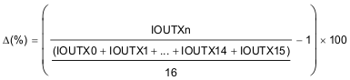
(1) The deviation of each outputs in same color group (OUTR0~15 or OUTG0~15 or OUTB0~15) from the average of same color group constant current. The deviation is calculated by the formula. (X = R or G or B, n = 0~15
(2) The deviation of the average of constant-current in each color group from the ideal constant-current value. (X = R or G or B) :
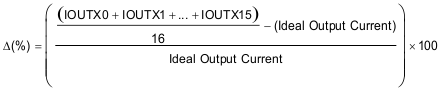
Ideal current is calculated by the following equation:

Ideal current is calculated by the following equation:
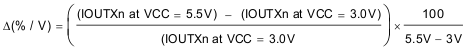
(3) Line regulation is calculated by the following equation. (X = R or G or B, n = 0~15):
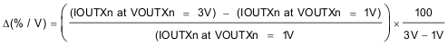
(4) Load regulation is calculated by the following equation. (X = R or G or B, n = 0~15):
7.6 Timing Requirements
At TA = –40°C to 85°C, unless otherwise noted.| MIN | TYP | MAX | UNIT | |||
|---|---|---|---|---|---|---|
| AC CHARACTERISTICS, VCC = 3 V to 5.5 V | ||||||
| tWH0 | Pulse duration | SCLK | 10 | ns | ||
| tWL0 | SCLK | 10 | ns | |||
| tWH1 | GCLK | 10 | ns | |||
| tWL1 | GCLK | 10 | ns | |||
| tWH2 | LAT | 10 | ns | |||
| tSU0 | Setup time | SIN – SCLK↑ | 2 | ns | ||
| tSU1 | LAT↑ – SCLK↑ | 3 | ns | |||
| tSU2 | LAT↓ – SCLK↑ , for WRTGS, WRTFC, and TMGST Command | 20 | ns | |||
| LAT↓ – SCLK↑ , for LATGS, READFC, and LINERESET Command | 80 | ns | ||||
| tSU3 | LAT↓ – GCLK↑ , for LATGS AND LINERESET Command | 30 | ns | |||
| tH0 | SCLK↑ – SIN | 2 | ns | |||
| tH1 | SCLK↑ – LAT↑ | 2 | ns | |||
| tH2 | SCLK↓ – LAT↓ | 2 | ns | |||
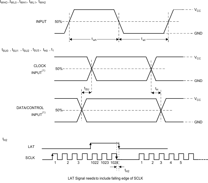 Figure 1. Input Timing
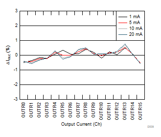
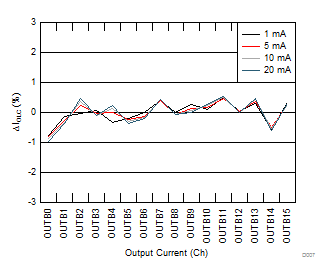
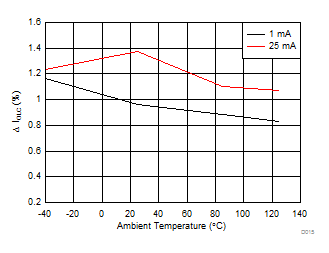
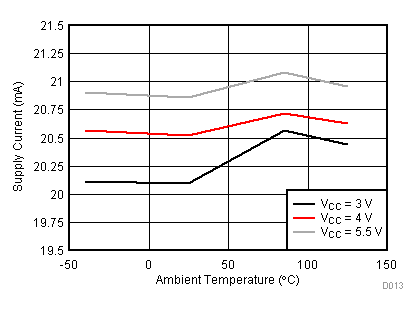
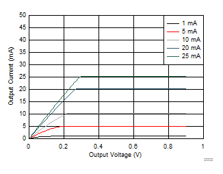
7.7 Typical Characteristics
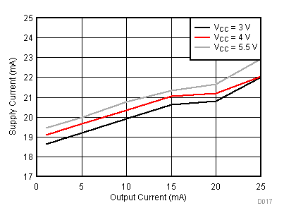
At VCC= 4V and TA = 25°C, unless otherwise noted.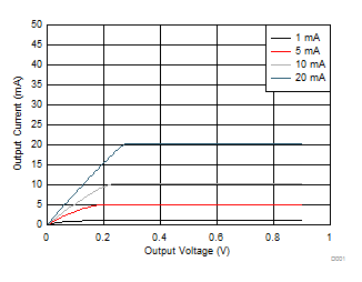
| VCC = 4 V |
| VCC = 4 V |
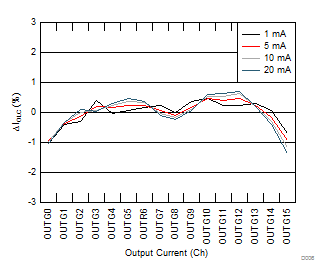
(Channel-to-Channel in RED color group)
| VCC = 4 V |
(Channel-to-Channel in BLUE color group)
| VCC=4V | VOUTXn=0.6V |
(Channel-to-Channel in GREEN color group)
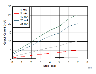
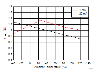
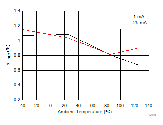
| GCLK=33MHz | VOUTXn=0.6V, | Output Current=10mA, | |
| GSXn=FFFFh, |
| VCC = 5 V |
| VCC = 4 V |
(Channel-to-Channel in GREEN color group)
| VCC=4V | VOUTXn=0.6V | |
(Channel-to-Channel in RED color group)
| VCC=4V | VOUTXn=0.6V |
(Channel-to-Channel in BLUE color group)
| VOUTXn=0.6V, | GCLK=33MHz, | GSXn=FFFFh, |