SLLSEY5F October 2017 – May 2022 TLIN1029-Q1
PRODUCTION DATA
- 1 Features
- 2 Applications
- 3 Description
- 4 Revision History
- 5 Description (continued)
- 6 Pin Configuration and Functions
- 7 Specifications
- 8 Parameter Measurement Information
-
9 Detailed Description
- 9.1 Overview
- 9.2 Functional Block Diagram
- 9.3
Feature Description
- 9.3.1 LIN (Local Interconnect Network) Bus
- 9.3.2 TXD (Transmit Input and Output)
- 9.3.3 RXD (Receive Output)
- 9.3.4 VSUP (Supply Voltage)
- 9.3.5 GND (Ground)
- 9.3.6 EN (Enable Input)
- 9.3.7 Protection Features
- 9.3.8 TXD Dominant Time Out (DTO)
- 9.3.9 Bus Stuck Dominant System Fault: False Wake-Up Lockout
- 9.3.10 Thermal Shutdown
- 9.3.11 Under Voltage on VSUP
- 9.3.12 Unpowered Device and LIN Bus
- 9.4 Device Functional Modes
- 10Application and Implementation
- 11Power Supply Recommendations
- 12Layout
- 13Device and Documentation Support
- 14Mechanical, Packaging, and Orderable Information
Package Options
Mechanical Data (Package|Pins)
Thermal pad, mechanical data (Package|Pins)
- DRB|8
Orderable Information
3 Description
The TLIN1029-Q1 is a local interconnect network (LIN) physical layer transceiver with integrated wake-up and protection features, compatible with LIN 2.0, LIN 2.1, LIN 2.2, LIN 2.2 A and ISO/DIS 17987–4.2 standards. LIN is a single-wire bidirectional bus typically used for in-vehicle networks using data rates up to 20 kbps. The TLIN1029-Q1 is designed to support 12-V applications with wider operating voltage and additional bus-fault protection.
The LIN receiver supports data rates up to 100 kbps for faster in-line programming. The TLIN1029-Q1 converts the data stream on the TXD input into a LIN bus signal using a current-limited wave-shaping driver which reduces electromagnetic emissions (EME). The receiver converts the data stream to logic level signals that are sent to the microprocessor through the open-drain RXD pin. Ultra-low current consumption is possible using the sleep mode which allows wake-up via LIN bus or EN pin.
| PART NUMBER | PACKAGE(1) | BODY SIZE (NOM) |
|---|---|---|
| TLIN1029-Q1 | SOIC (D) (8) | 4.90 mm x 3.91 mm |
| VSON (DRB) (8) | 3.00 mm x 3.00 mm |
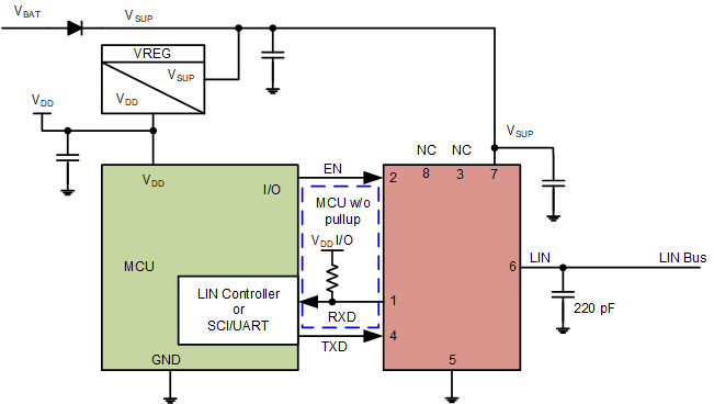
 Simplified Schematics, Responder Mode