SBOS832A July 2017 – August 2017 TLV07
PRODUCTION DATA.
- 1 Features
- 2 Applications
- 3 Description
- 4 Revision History
- 5 Pin Configuration and Functions
- 6 Specifications
- 7 Detailed Description
- 8 Application and Implementation
- 9 Power Supply Recommendations
- 10Layout
- 11Device and Documentation Support
- 12Mechanical, Packaging, and Orderable Information
Package Options
Mechanical Data (Package|Pins)
- D|8
Thermal pad, mechanical data (Package|Pins)
Orderable Information
8 Application and Implementation
NOTE
Information in the following applications sections is not part of the TI component specification, and TI does not warrant its accuracy or completeness. TI’s customers are responsible for determining suitability of components for their purposes. Customers should validate and test their design implementation to confirm system functionality.
8.1 Application Information
The TLV07 op amp provides high overall performance in a large number of general-purpose applications. As with all amplifiers, applications with noisy or high-impedance power supplies require decoupling capacitors placed close to the device pins. In most cases, 0.1-µF capacitors are adequate. Follow the additional recommendations in Layout Guidelines to achieve the maximum performance from this device. Many applications may introduce capacitive loading to the output of the amplifier, potentially causing instability. Add an isolation resistor between the amplifier output and the capacitive load to stabilize the amplifier. Typical Application shows the design process for selecting this resistor.
8.2 Typical Application
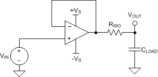
This circuit can drive capacitive loads such as cable shields, reference buffers, MOSFET gates, and diodes. The circuit uses an isolation resistor (RISO) to stabilize the output of an op amp. RISO modifies the open-loop gain of the system to ensure the circuit has sufficient phase margin.
 Figure 35. Unity-Gain Buffer With RISO Stability Compensation
8.2.1 Design Requirements
The design requirements are:
- Supply voltage: 30 V (±15 V)
- Capacitive loads: 100 pF, 1000 pF, 0.01 μF, 0.1 μF, and 1 μF
- Phase margin: 45° and 60°
8.2.2 Detailed Design Procedure
Figure 35 shows a unity-gain buffer driving a capacitive load. Equation 1 shows the transfer function for the circuit in Figure 35. Figure 35 does not show the open-loop output resistance of the op amp (RO).

The transfer function shown in Equation 1 has a pole and a zero. (RO + RISO) and CLOAD determine the frequency of the pole (fp). The RISO and CLOAD components determine the frequency of the zero (fz). A stable system is obtained by selecting RISO such that the rate of closure (ROC) between the open-loop gain (AOL) and 1/β is 20 dB/decade.
ROC stability analysis is typically simulated. The validity of the analysis depends on multiple factors, especially the accurate modeling of R O. In addition to simulating the ROC, a robust stability analysis includes a measurement of overshoot percentage and ac gain peaking of the circuit using a function generator, oscilloscope, and gain and phase analyzer. These measurements then calculate phase margin. Table 2 shows the overshoot percentage and ac gain peaking that correspond to phase margins of 45° and 60°. For more details on this design and other alternative devices that can be used in place of the TLV07, see Capacitive Load Drive Solution Using an Isolation Resistor
Table 2. Phase Margin versus Overshoot and AC Gain Peaking
| PHASE MARGIN | OVERSHOOT | AC GAIN PEAKING |
|---|---|---|
| 45° | 23.3% | 2.35 dB |
| 60° | 8.8% | 0.28 dB |
8.2.3 Application Curve
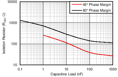
The values of RISO that yield phase margins of 45° and 60° for various capacitive loads are determined using the described methodology Figure 36 shows the results.
 Figure 36. Isolation Resistor Required for Various Capacitive Loads to Achieve a Target Phase Margin