SLVS561O December   2004  – June 2025 TLV1117

PRODUCTION DATA  

  1.   1
  2. Features
  3. Applications
  4. Description
  5. Pin Configuration and Functions
  6. Specifications
    1. 5.1 Absolute Maximum Ratings
    2. 5.2 ESD Ratings
    3. 5.3 Recommended Operating Conditions
    4. 5.4 Thermal Information (Legacy Chip)
    5. 5.5 Thermal Information (New Chip)
    6. 5.6 Electrical Characteristics
    7. 5.7 Typical Characteristics
  7. Detailed Description
    1. 6.1 Overview
    2. 6.2 Functional Block Diagrams
    3. 6.3 Feature Description
      1. 6.3.1 Dropout Voltage (Fixed Output, New Chip)
      2. 6.3.2 Foldback Current Limit (Fixed Output, New Chip)
      3. 6.3.3 Undervoltage Lockout (Fixed Output, New Chip)
      4. 6.3.4 Thermal Shutdown (Fixed Output, New Chip)
      5. 6.3.5 Load Regulation (Adjustable Output, New Chip)
    4. 6.4 Device Functional Modes
      1. 6.4.1 Device Functional Mode Comparison (Fixed Output, New Chip)
      2. 6.4.2 Normal Operation (Fixed Output)
      3. 6.4.3 Dropout Operation (Fixed Output, New Chip)
      4. 6.4.4 Protection Diodes (Adjustable Output, New Chip)
  8. Application and Implementation
    1. 7.1 Application Information
      1. 7.1.1 Recommended Capacitor Types (Fixed Output, New Chip)
      2. 7.1.2 Input and Output Capacitor Requirements (Fixed Output, New Chip)
      3. 7.1.3 Reverse Current (Fixed Output, New Chip)
      4. 7.1.4 Power Dissipation (Fixed Output, New Chip)
      5. 7.1.5 Estimating Junction Temperature (Fixed Output, New Chip)
    2. 7.2 Typical Application (Adjustable Output)
      1. 7.2.1 Design Requirements (Adjustable Output)
      2. 7.2.2 Detailed Design Procedure
        1. 7.2.2.1 Detailed Design Procedure (Fixed Output, New Chip)
        2. 7.2.2.2 Detailed Design Procedure (Adjustable Output)
      3. 7.2.3 Application Curves
    3. 7.3 Power Supply Recommendations
    4. 7.4 Layout
      1. 7.4.1 Layout Guidelines
      2. 7.4.2 Layout Example
  9. Device and Documentation Support
    1. 8.1 Device Support
      1. 8.1.1 Device Nomenclature
    2. 8.2 Receiving Notification of Documentation Updates
    3. 8.3 Support Resources
    4. 8.4 Trademarks
    5. 8.5 Electrostatic Discharge Caution
    6. 8.6 Glossary
  10. Revision History
  11. 10Mechanical, Packaging, and Orderable Information

Package Options

Refer to the PDF data sheet for device specific package drawings

Mechanical Data (Package|Pins)
  • KVU|3
  • DRJ|8
  • DCY|4
  • KCS|3
  • KTT|3
Thermal pad, mechanical data (Package|Pins)
Orderable Information

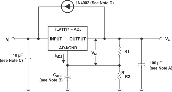
Typical Application (Adjustable Output)

TLV1117 Basic
                    Adjustable Regulator Figure 7-2 Basic Adjustable Regulator
Note:

The Design Requirements (Adjustable Output) section lists details for notes referenced in Figure 7-2.

The adjustable version of the TLV1117 takes a 2.7V to 15V input. The VREF voltage refers to the voltage between the output and the ADJUST pin, typically 1.25V. The VREF voltage causes current to flow across R1, which is the same current that flows across R2 (minus the negligible 50µA IADJ). Therefore, adjust R2 to create a larger voltage drop from GND and set the output voltage. The output voltage equation is described in the Detailed Design Procedure (Adjustable Output) section.