SBVS160C May   2011  – January 2023 TLV1117LV

PRODUCTION DATA  

  1. Features
  2. Applications
  3. Description
  4. Revision History
  5. Pin Configuration and Functions
  6. Specifications
    1. 6.1 Absolute Maximum Ratings
    2. 6.2 ESD Ratings
    3. 6.3 Recommended Operating Conditions
    4. 6.4 Thermal Information
    5. 6.5 Electrical Characteristics
    6. 6.6 Typical Characteristics
  7. Detailed Description
    1. 7.1 Overview
    2. 7.2 Functional Block Diagram
    3. 7.3 Feature Description
      1. 7.3.1 Internal Current Limit
      2. 7.3.2 Dropout Voltage
      3. 7.3.3 Undervoltage Lockout
    4. 7.4 Device Functional Modes
      1. 7.4.1 Normal Operation
      2. 7.4.2 Dropout Operation
  8. Application and Implementation
    1. 8.1 Application Information
    2. 8.2 Typical Application
      1. 8.2.1 Design Requirements
      2. 8.2.2 Detailed Design Procedure
        1. 8.2.2.1 Input and Output Capacitor Requirements
        2. 8.2.2.2 Transient Response
      3. 8.2.3 Application Curves
    3. 8.3 Best Design Practices
    4. 8.4 Power Supply Recommendations
    5. 8.5 Layout
      1. 8.5.1 Layout Guidelines
        1. 8.5.1.1 Thermal Protection
        2. 8.5.1.2 Power Dissipation
      2. 8.5.2 Layout Example
  9. Device and Documentation Support
    1. 9.1 Device Support
      1. 9.1.1 Development Support
        1. 9.1.1.1 Evaluation Module
        2. 9.1.1.2 Spice Models
      2. 9.1.2 Device Nomenclature
    2. 9.2 Documentation Support
      1. 9.2.1 Related Documentation
    3. 9.3 Receiving Notification of Documentation Updates
    4. 9.4 Support Resources
    5. 9.5 Trademarks
    6. 9.6 Electrostatic Discharge Caution
    7. 9.7 Glossary
  10. 10Mechanical, Packaging, and Orderable Information

Package Options

Mechanical Data (Package|Pins)
Thermal pad, mechanical data (Package|Pins)
Orderable Information

Typical Characteristics

at VIN = VOUT(nom) + 1.5 V, IOUT = 10 mA, COUT = 1.0 μF, and TA = 25°C (unless otherwise noted)
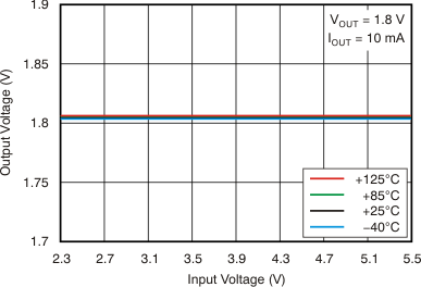
GUID-6DF5E9D9-1F1B-48AA-AABD-4C6A9941151C-low.gif
 
Figure 6-1 Line Regulation
GUID-D3BE5486-DE44-4E9E-86E2-27FAFBBDF041-low.gif
 
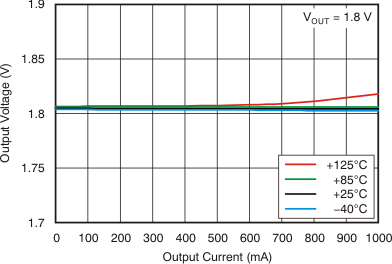
Figure 6-3 Load Regulation
GUID-DF09872A-0F1B-491E-B7EF-010FCAF71A43-low.gif
 
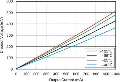
Figure 6-5 Dropout Voltage vs Output Current
GUID-2859217A-67CB-4041-A5D4-0ECB183BC5D5-low.gif
 
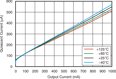
Figure 6-7 Quiescent Current vs Load
GUID-503C90CB-0796-44D9-B7B1-20CD77C5588A-low.gif
 
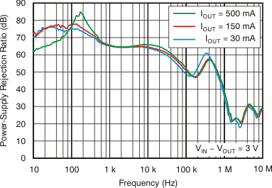
Figure 6-9 Power-Supply Rejection Ratio vs Frequency
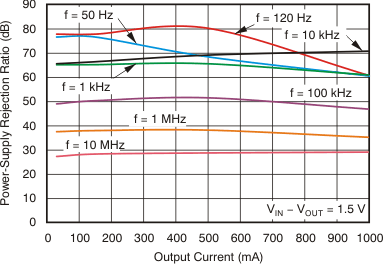
GUID-D26A5707-2965-4478-9F99-82B093889BA9-low.gif
 
Figure 6-11 Power-Supply Rejection Ratio vs Output Current
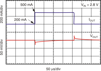
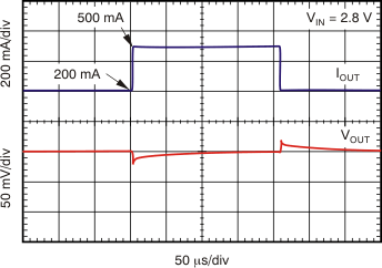
GUID-0F9ABBFD-F708-405E-BD28-7316F8DF21B2-low.gif
COUT = 1 μF
Figure 6-13 Load Transient Response 200 mA to 500 mA
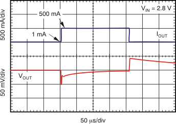
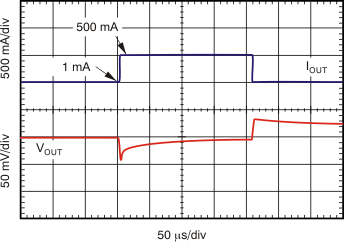
GUID-8154773E-608B-4129-86DA-AFF3853F9A6B-low.gif
COUT = 1 μF
Figure 6-15 Load Transient Response 1 mA to 500 mA
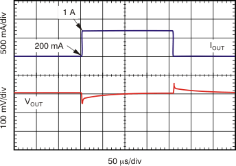
GUID-4D72A9FF-D8E8-4F76-A083-1518994FAC19-low.gif
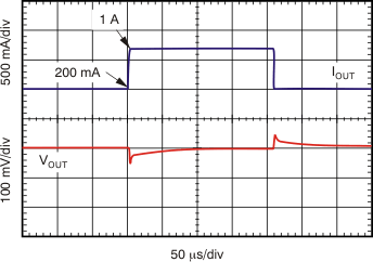
COUT = 1 μF
Figure 6-17 Load Transient Response 200 mA to 1 A
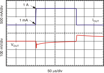
GUID-09AEF0E0-9308-487B-A240-FA7026A44659-low.gif
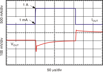
COUT = 1 μF
Figure 6-19 Load Transient Response 1 mA to 1 A
GUID-01857444-2DF3-4AE5-B974-7ABC1155CDC0-low.gif
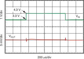
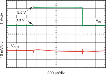
VOUT = 1.8 V, IOUT = 10 mA
Figure 6-21 Line Transient Response
GUID-0F9A5E6C-FCD2-4236-BD1E-FC8FA81124FA-low.gif
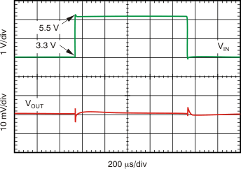
VOUT = 1.8 V, IOUT = 1 A
Figure 6-23 Line Transient Response
GUID-90F2E1F6-2C4E-4CAC-8E57-3EFFDC25654A-low.gif
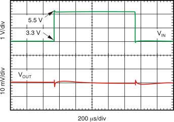
VOUT = 1.8 V, IOUT = 500 mA
Figure 6-25 Line Transient Response
GUID-72C75260-6E75-495C-98DF-DC26FBEB912A-low.gif
 
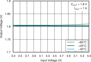
Figure 6-2 Line Regulation
GUID-00A26EBC-175D-4D0C-B4F3-FF4E0F004A25-low.gif
 
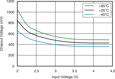
Figure 6-4 Dropout Voltage vs Input Voltage
GUID-F855C67D-6250-42A3-9262-267FEFC5C8C3-low.gif
 
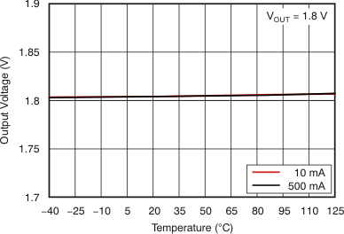
Figure 6-6 Output Voltage vs Temperature
GUID-0288976C-1827-4AB4-AF76-DD1DD224FB10-low.gif
 
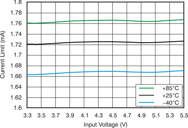
Figure 6-8 Current Limit vs Input Voltage
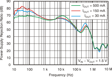
GUID-29212BF8-3DD1-49AF-9EF7-A759870B3F32-low.gif
 
Figure 6-10 Power-Supply Rejection Ratio vs Frequency
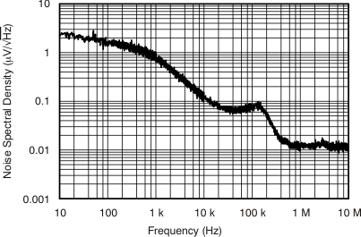
GUID-87B601EC-5C98-4B67-B539-92992BAA5B06-low.gif
 
Figure 6-12 Spectral Noise Density vs Frequency
GUID-CFB85047-4481-4EA6-B577-41FAC90C1B36-low.gif
COUT = 10 μF
Figure 6-14 Load Transient Response 200 mA to 500 mA
GUID-E821A1A6-3262-43A6-A965-1884C8956C5A-low.gif
COUT = 10 μF
Figure 6-16 Load Transient Response 1 mA to 500 mA
GUID-865C8F47-1111-4D7F-AF9B-BD2C98C88EBE-low.gif
COUT = 10 μF
Figure 6-18 Load Transient Response 200 mA to 1 A
GUID-8967599A-6246-4BF4-A7C6-044EB35D01C7-low.gif
COUT = 10 μF
Figure 6-20 Load Transient Response 1 mA to 1 A
GUID-A6497316-4C7F-496C-BC49-90205652D2A2-low.gif
VOUT = 1.8 V, IOUT = 500 mA
Figure 6-22 Line Transient Response
GUID-F61D8564-9B0B-4817-9A1C-BD479D52201A-low.gif
VOUT = 1.8 V, IOUT = 10 mA
Figure 6-24 Line Transient Response
GUID-6DE96A17-A7BD-4112-8DDD-787727AA99C8-low.gif
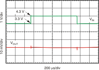
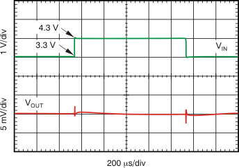
VOUT = 1.8 V, IOUT = 1 A
Figure 6-26 Line Transient Response