SBOS782A November   2016  – May 2018 TLV170 , TLV2170 , TLV4170

PRODUCTION DATA.  

  1. Features
  2. Applications
    1.     Smallest Packaging for 36-V Operational Amplifiers
  3. Description
  4. Revision History
  5. Pin Configuration and Functions
    1.     Pin Functions: TLV170
    2.     Pin Functions: TLV2170
    3.     Pin Functions: TLV4170
  6. Specifications
    1. 6.1 Absolute Maximum Ratings
    2. 6.2 ESD Ratings
    3. 6.3 Recommended Operating Conditions
    4. 6.4 Thermal Information: TLV170
    5. 6.5 Thermal Information: TLV2170
    6. 6.6 Thermal Information: TLV4170
    7. 6.7 Electrical Characteristics
    8. 6.8 Typical Characteristics: Table of Graphs
    9. 6.9 Typical Characteristics
  7. Detailed Description
    1. 7.1 Overview
    2. 7.2 Functional Block Diagram
    3. 7.3 Feature Description
      1. 7.3.1 Operating Characteristics
      2. 7.3.2 Phase-Reversal Protection
      3. 7.3.3 Electrical Overstress
      4. 7.3.4 Capacitive Load and Stability
    4. 7.4 Device Functional Modes
      1. 7.4.1 Common-Mode Voltage Range
      2. 7.4.2 Overload Recovery
  8. Application and Implementation
    1. 8.1 Application Information
    2. 8.2 Typical Application
      1. 8.2.1 Design Requirements
      2. 8.2.2 Detailed Design Procedure
      3. 8.2.3 Application Curve
  9. Power Supply Recommendations
  10. 10Layout
    1. 10.1 Layout Guidelines
    2. 10.2 Layout Example
  11. 11Device and Documentation Support
    1. 11.1 Device Support
      1. 11.1.1 Development Support
        1. 11.1.1.1 TINA-TI™ (Free Software Download)
        2. 11.1.1.2 DIP Adapter EVM
        3. 11.1.1.3 Universal Op Amp EVM
        4. 11.1.1.4 TI Precision Designs
        5. 11.1.1.5 WEBENCH Filter Designer
    2. 11.2 Documentation Support
      1. 11.2.1 Related Documentation
    3. 11.3 Related Links
    4. 11.4 Receiving Notification of Documentation Updates
    5. 11.5 Community Resources
    6. 11.6 Trademarks
    7. 11.7 Electrostatic Discharge Caution
    8. 11.8 Glossary
  12. 12Mechanical, Packaging, and Orderable Information

Package Options

Mechanical Data (Package|Pins)
Thermal pad, mechanical data (Package|Pins)
Orderable Information

Typical Characteristics

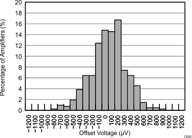
TLV170 TLV2170 TLV4170 G001_sbos782.gif
Distribution taken from 400 amplifiers
Figure 1. Offset Voltage Production Distribution
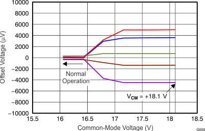
TLV170 TLV2170 TLV4170 G005_sbos782.gif
5 typical units shown
Figure 3. Offset Voltage vs Common-Mode Voltage
(Upper Stage)
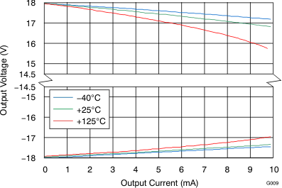
TLV170 TLV2170 TLV4170 G009_BOS557.gif
Figure 5. Output Voltage Swing vs Output Current (Maximum Supply)
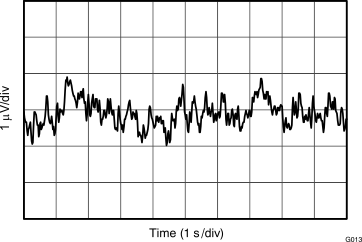
TLV170 TLV2170 TLV4170 G013_sbos782.gif
Figure 7. 0.1-Hz to 10-Hz Noise
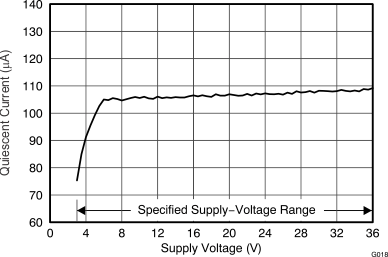
TLV170 TLV2170 TLV4170 G018_sbos782.gif
Figure 9. Quiescent Current vs Supply Voltage
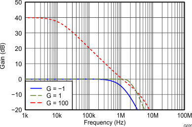
TLV170 TLV2170 TLV4170 G020_BOS557.gif
Figure 11. Closed-Loop Gain vs Frequency
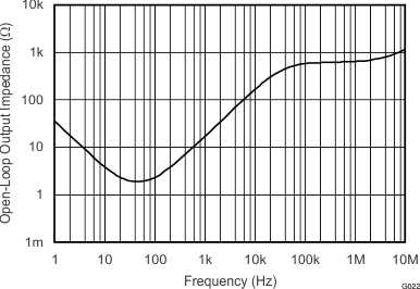
TLV170 TLV2170 TLV4170 G022_sbos782.gif
Figure 13. Open-Loop Output Impedance vs Frequency
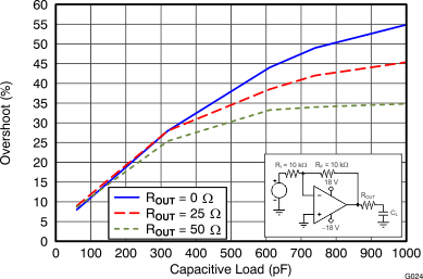
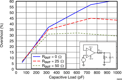
TLV170 TLV2170 TLV4170 tc_small-sig_ovrst_cap_load_g-1_bos782.gif
100-mV output step, RL = 10 kΩ, G = –1
Figure 15. Small-Signal Overshoot vs Capacitive Load
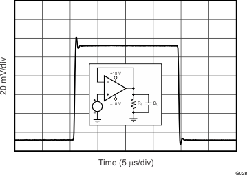
TLV170 TLV2170 TLV4170 tc_small-sig_step_resp_g1_bos782.gif
RL = 10 kΩ, CL = 10 pF, G = +1
Figure 17. Small-Signal Step Response (100 mV)
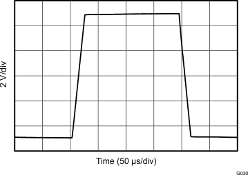
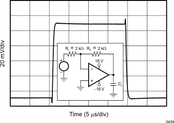
TLV170 TLV2170 TLV4170 G030_SBOS782.gif
G = +1, RL = 10 kΩ, CL = 10 pF
Figure 19. Large-Signal Step Response
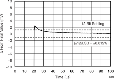
TLV170 TLV2170 TLV4170 G032_BOS557.gif
10-V positive step, G = +1
Figure 21. Large-Signal Settling Time
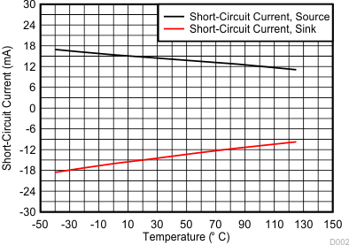
TLV170 TLV2170 TLV4170 G034_SBOS782.gif
Figure 23. Short-Circuit Current vs Temperature
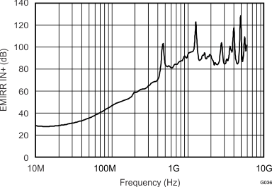
TLV170 TLV2170 TLV4170 G036_sbos782.gif
PRP = –10 dBm, VS = ±18 V, VCM = 0 V
Figure 25. EMIRR IN+ vs Frequency
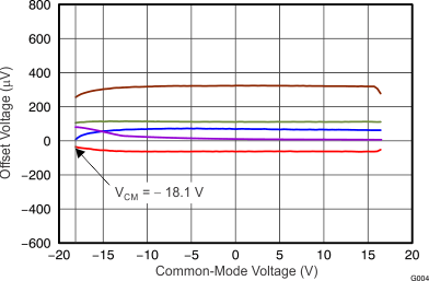
TLV170 TLV2170 TLV4170 G004_sbos782.gif
5 typical units shown
Figure 2. Offset Voltage vs Common-Mode Voltage
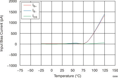
TLV170 TLV2170 TLV4170 G008_BOS557.gif
Figure 4. Input Bias Current vs Temperature
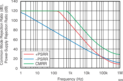
TLV170 TLV2170 TLV4170 G010_BOS557.gif
Figure 6. CMRR and PSRR vs Frequency
(Referred-to Input)
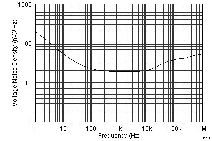
TLV170 TLV2170 TLV4170 G014_BOS557.png
Figure 8. Input Voltage Noise Spectral Density vs Frequency
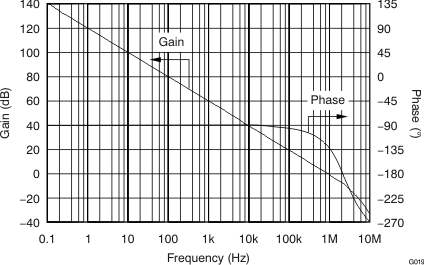
TLV170 TLV2170 TLV4170 G019_BOS557.gif
Figure 10. Open-Loop Gain and Phase vs Frequency
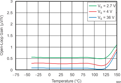
TLV170 TLV2170 TLV4170 G021_sbos782.gif
Figure 12. Open-Loop Gain vs Temperature
TLV170 TLV2170 TLV4170 tc_small-sig_ovrst_cap_load_g1_bos782.gif
100-mV output step, RL = 10 kΩ, G = +1
Figure 14. Small-Signal Overshoot vs Capacitive Load
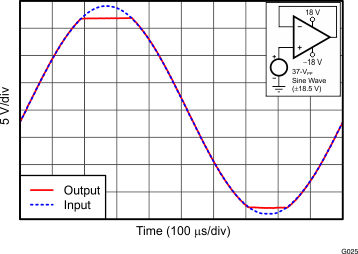
TLV170 TLV2170 TLV4170 tc_no_phase_reverse_bos782.gif
Figure 16. No Phase Reversal
TLV170 TLV2170 TLV4170 tc_small-sig_step_resp_g-1_bos782.gif
RL = 10 kΩ, CL = 10 pF, G = –1
Figure 18. Small-Signal Step Response (100 mV)
TLV170 TLV2170 TLV4170 G031_sbos782.gif
G = –1, RL = 10 kΩ, CL = 10 pF
Figure 20. Large-Signal Step Response
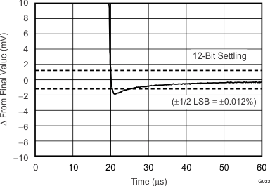
TLV170 TLV2170 TLV4170 G033_sbos782.gif
10-V negative step, G = –1
Figure 22. Large-Signal Settling Time
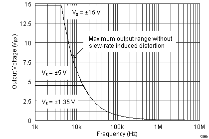
TLV170 TLV2170 TLV4170 G035_BOS557.png
Figure 24. Maximum Output Voltage vs Frequency