SNOSD50A December   2018  – January 2020 TLV1805

PRODUCTION DATA.  

  1. Features
  2. Applications
  3. Description
    1.     Device Images
      1.      Reverse Current Protection Using an N-Channel MOSFET
      2.      Reverse Current & Overvoltage Protection Using P-Channel MOSFETs
  4. Revision History
  5. Pin Configuration and Functions
    1.     Pin Functions
  6. Specifications
    1. 6.1 Absolute Maximum Ratings
    2. 6.2 ESD Ratings
    3. 6.3 Recommended Operating Conditions
    4. 6.4 Thermal Information
    5. 6.5 Electrical Characteristics
    6. 6.6 Switching Characteristics
    7. 6.7 Typical Characteristics
  7. Detailed Description
    1. 7.1 Overview
    2. 7.2 Functional Block Diagram
    3. 7.3 Feature Description
      1. 7.3.1 Rail to Rail Inputs
      2. 7.3.2 Power On Reset
      3. 7.3.3 High Power Push-Pull Output
      4. 7.3.4 Shutdown Function
      5. 7.3.5 Internal Hysteresis
    4. 7.4 Device Functional Modes
      1. 7.4.1 External Hysteresis
        1. 7.4.1.1 Inverting Comparator With Hysteresis
        2. 7.4.1.2 Noninverting Comparator With Hysteresis
  8. Application and Implementation
    1. 8.1 Application Information
    2. 8.2 Typical Applications
      1. 8.2.1 Design Requirements
      2. 8.2.2 Detailed Design Procedure
      3. 8.2.3 Application Curve
      4. 8.2.4 Reverse Current Protection Using MOSFET and TLV1805
        1. 8.2.4.1 Minimum Reverse Current
        2. 8.2.4.2 N-Channel Reverse Current Protection Circuit
          1. 8.2.4.2.1 N-Channel Oscillator Circuit
      5. 8.2.5 P-Channel Reverse Current Protection Circuit
      6. 8.2.6 P-Channel Reverse Current Protection With Overvotlage Protection
      7. 8.2.7 ORing MOSFET Controller
  9. Power Supply Recommendations
  10. 10Layout
    1. 10.1 Layout Guidelines
    2. 10.2 Layout Example
  11. 11Device and Documentation Support
    1. 11.1 Documentation Support
      1. 11.1.1 Related Documentation
    2. 11.2 Receiving Notification of Documentation Updates
    3. 11.3 Support Resources
    4. 11.4 Trademarks
    5. 11.5 Electrostatic Discharge Caution
    6. 11.6 Glossary
  12. 12Mechanical, Packaging, and Orderable Information

Package Options

Mechanical Data (Package|Pins)
Thermal pad, mechanical data (Package|Pins)
Orderable Information

Internal Hysteresis

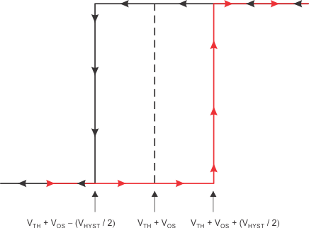
The TLV1805 contains 14mV of internal hysteresis.

The hysteresis transfer curve is shown in Figure 63. This curve is a function of three components: VTH, VOS, and VHYST:

  • VTH is the actual set voltage or threshold trip voltage.
  • VOS is the internal offset voltage between VIN+ and VIN–. This voltage is added to VTH to form the actual trip point at which the comparator must respond to change output states.
  • VHYST is the internal hysteresis (or trip window) that is designed to reduce comparator sensitivity to noise
    (14 mV for the TLV1805).
TLV1805 ai_hyst_transfer_bos694.gifFigure 63. Hysteresis Transfer Curve