SBOS753B June 2016 – February 2017 TLV2313 , TLV313 , TLV4313
PRODUCTION DATA.
- 1 Features
- 2 Applications
- 3 Description
- 4 Revision History
- 5 Device Comparison Table
- 6 Pin Configuration and Functions
-
7 Specifications
- 7.1 Absolute Maximum Ratings
- 7.2 ESD Ratings
- 7.3 Recommended Operating Conditions
- 7.4 Thermal Information: TLV313
- 7.5 Thermal Information: TLV2313
- 7.6 Thermal Information: TLV4313
- 7.7 Electrical Characteristics: 5.5 V
- 7.8 Electrical Characteristics: 1.8 V
- 7.9 Typical Characteristics: Table of Graphs
- 7.10 Typical Characteristics
- 8 Detailed Description
- 9 Application and Implementation
- 10Power Supply Recommendations
- 11Layout
- 12Device and Documentation Support
- 13Mechanical, Packaging, and Orderable Information
Package Options
Mechanical Data (Package|Pins)
Thermal pad, mechanical data (Package|Pins)
Orderable Information
1 Features
- Precision Amplifier for Cost-Sensitive Systems
- Low IQ: 65 µA/ch
- Wide Supply Range: 1.8 V to 5.5 V
- Low Noise: 26 nV/√Hz at 1 kHz
- Gain Bandwidth: 1 MHz
- Rail-to-Rail Input/Output
- Low Input Bias Current: 1 pA
- Low Offset Voltage: 0.75 mV
- Unity-Gain Stable
- Internal RF/EMI Filter
- Extended Temperature Range:
–40°C to +125°C
2 Applications
- Medical and Healthcare
- Fitness and Wearable Electronics
- Utility Metering (Heat, Water, Energy)
- Building Automation Equipment
- Currency Counters
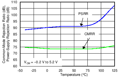
CMRR and PSRR vs Temperature

3 Description
The TLV313 family of single-, dual-, and quad-channel precision operational amplifiers combine low power consumption with good performance. This makes them suitable for a wide range of applications, such as wearables, utility metering, building automation, currency counters and more. The family features rail-to-rail input and output (RRIO) swings, low quiescent current (65 μA, typical), wide bandwidth (1 MHz) and very low noise (26 nV/√Hz at 1 kHz), making it attractive for a variety of battery-powered applications that require a good balance between cost and performance. Further, low-input-bias current enables these devices to be used in applications with megaohm source impedances.
The robust design of the TLV313 devices provides ease-of-use to the circuit designer: unity-gain stability with capacitive loads of up to 150 pF, integrated RF/EMI rejection filter, no phase reversal in overdrive conditions, and high electrostatic discharge (ESD) protection (4-kV HBM).
The devices are optimized for operation at voltages as low as +1.8 V (±0.9 V) and up to +5.5 V (±2.75 V), and are specified over the extended temperature range of –40°C to +125°C.
The single-channel TLV313 device is available in both SC70-5 and SOT23-5 packages. The dual-channel TLV2313 device is offered in SOIC-8 and VSSOP-8 packages, and the quad-channel TLV4313 device is offered in a TSSOP-14 package.
Device Information(1)
| PART NUMBER | PACKAGE | BODY SIZE (NOM) |
|---|---|---|
| TLV313 | SC70 (5) | 2.00 mm × 1.25 mm |
| SOT23 (5) | 2.90 mm × 1.60 mm | |
| TLV2313 | SOIC (8) | 4.90 mm × 3.91 mm |
| VSSOP (8) | 3.00 mm × 3.00 mm | |
| TLV4313 | TSSOP (14) | 5.00 mm × 4.40 mm |
- For all available packages, see the orderable addendum at the end of the data sheet.
4 Revision History
Changes from A Revision (June 2016) to B Revision
- Changed pin assignment for DCK packageGo
Changes from * Revision (June 2016) to A Revision