SBOS751 December 2015 TLV2333 , TLV333 , TLV4333
PRODUCTION DATA.
- 1 Features
- 2 Applications
- 3 Description
- 4 Revision History
- 5 Device Comparison Table
- 6 Pin Configuration and Functions
- 7 Specifications
- 8 Detailed Description
- 9 Application and Implementation
- 10Power Supply Recommendations
- 11Layout
- 12Device and Documentation Support
- 13Mechanical, Packaging, and Orderable Information
Package Options
Mechanical Data (Package|Pins)
Thermal pad, mechanical data (Package|Pins)
Orderable Information
9 Application and Implementation
NOTE
Information in the following applications sections is not part of the TI component specification, and TI does not warrant its accuracy or completeness. TI’s customers are responsible for determining suitability of components for their purposes. Customers should validate and test their design implementation to confirm system functionality.
9.1 System Examples
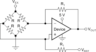
Figure 21 shows the basic configuration for a bridge amplifier.
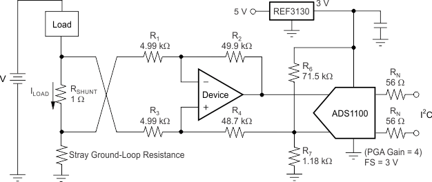
A low-side current shunt monitor is shown in Figure 22.
 Figure 21. Single Op Amp Bridge Amplifier

NOTE:
1% resistors provide adequate common-mode rejection at small ground-loop errors.RN are operational resistors used to isolate the ADS1100 from the noise of the digital I2C bus. Because the ADS1100 is a 16-bit converter, a precise reference is essential for maximum accuracy. If absolute accuracy is not required, and the 5-V power supply is sufficiently stable, the REF3130 can be omitted.
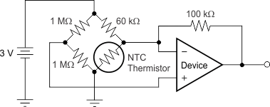
Figure 23 shows the TLV333 in a typical thermistor circuit.
 Figure 23. Thermistor Measurement