SGLS244B May 2004 – December 2016 TLV2371-Q1 , TLV2372-Q1 , TLV2374-Q1
PRODUCTION DATA.
- 1 Features
- 2 Applications
- 3 Description
- 4 Revision History
- 5 Device Comparison Table
- 6 Pin Configuration and Functions
- 7 Specifications
- 8 Detailed Description
- 9 Application and Implementation
- 10Power Supply Recommendations
- 11Layout
- 12Device and Documentation Support
- 13Mechanical, Packaging, and Orderable Information
Package Options
Refer to the PDF data sheet for device specific package drawings
Mechanical Data (Package|Pins)
- D|8
Thermal pad, mechanical data (Package|Pins)
Orderable Information
9 Application and Implementation
NOTE
Information in the following applications sections is not part of the TI component specification, and TI does not warrant its accuracy or completeness. TI’s customers are responsible for determining suitability of components for their purposes. Customers should validate and test their design implementation to confirm system functionality.
9.1 Application Information
When designing for low power, choose system components carefully. To minimize current consumption, select large-value resistors. Any resistors can react with stray capacitance in the circuit and the input capacitance of the operational amplifier. These parasitic RC combinations can affect the stability of the overall system. Use of a feedback capacitor assures stability and limits overshoot or gain peaking.
9.2 Typical Applications
9.2.1 High-Side Current Monitor
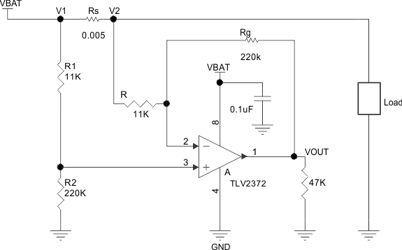
The TLV237x-Q1 is rail-to-rail input and output capability and up to 16-V supply voltage. That makes the device suitable in body control model applications and more specific high-side current sensing. The input common mode is at the supply voltage so there is no limitation in differential gain.
 Figure 32. Application Circuit
9.2.1.1 Design Requirements
For this design example, use these parameters listed in Table 2 as the input parameters.
Table 2. Design Parameters
| PARAMETER | VALUE | |
|---|---|---|
| VBAT | Battery voltage | 12 V |
| RSENSE | 0.05 Ω | |
| ILOAD | Load current | 0 A to 10 A |
| Operational amplifier | Set in differential configuration with gain = 20 |
|
9.2.1.2 Detailed Design Procedure
This circuit is designed for measuring the high-side current in automotive body control modules with a 12-V battery or similar applications. The operational amplifier is set as differential with an external resistor network.
9.2.1.2.1 Differential Amplifier Equations
Equation 1 and Equation 2 are used to calculate VOUT.


In an ideal case, R1 = R, R2 = Rg, and VOUT can then be calculated using Equation 3.

However, as the resistors have tolerances, they cannot be perfectly matched.

By developing the equations and neglecting the second order, the worst case is when the tolerances add up. This is shown by Equation 9.

where
- Tol = 0.01 for 1%
- Tol = 0.001 for 0.1%
If the resistors are perfectly matched, then Tol = 0 and Vout is calculated using Equation 10.

The highest error is from the common mode in Equation 11.

Gain of 20, Rg/R = 20, and Tol = 1% in Equation 12.
When the gain of 20 and Tol = 0.1%, the common-mode error = 45.7 mV.
The resistors were chosen from 1% batches.
- R1 and R are 11 kΩ
- R2 and Rg are 220 kΩ
Ideal Gain = 220 / 11 = 20
The measured value of the resistors:
- R1 = 10.97 kΩ
- R = 10.96 kΩ
- R2 = 220.23 kΩ
- Rg = 220.15 kΩ
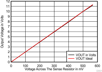
9.2.1.3 Application Curve
 Figure 33. Output Voltage vs Differential Input in High Current Sensing
9.2.2 Inverting Amplifier
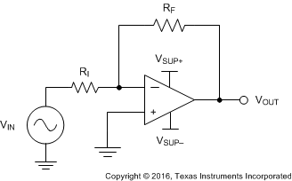
A typical application for an operational amplifier is an inverting amplifier, as shown in Figure 34. An inverting amplifier takes a positive voltage on the input and outputs a signal inverted to the input, making a negative voltage of the same magnitude. In the same manner, the amplifier also makes negative input voltages positive on the output. In addition, amplification can be added by selecting the input resistor RI and the feedback resistor RF.
 Figure 34. Amplifier Schematic
9.2.3 Design Requirements
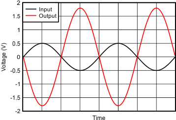
The supply voltage must be chosen to be larger than the input voltage range and the desired output range. The limits of the input common-mode range (VCM) and the output voltage swing to the rails (VO) must also be considered. For instance, this application scales a signal of ±0.5 V (1 V) to ±1.8 V (3.6 V). Setting the supply at ±2.5 V is sufficient to accommodate this application.
9.2.4 Detailed Design Procedure
Determine the gain required by the inverting amplifier using Equation 13 and Equation 14.


When the desired gain is determined, choose a value for RI or RF. Choosing a value in the kΩ range is desirable for general-purpose applications because the amplifier circuit uses currents in the milliamp range. This milliamp current range ensures the device does not draw too much current. The trade-off is that large resistors (hundreds of kΩ) draw the smallest current but generate the highest noise. Small resistors (hundreds of Ω) generate low noise but draw high current. This example uses 10 kΩ for RI, meaning 36 kΩ is used for RF. These values are determined by Equation 15.

9.2.5 Application Curve
 Figure 35. Inverting Amplifier Input and Output