SLOS270F March 2001 – August 2016 TLV2370 , TLV2371 , TLV2372 , TLV2373 , TLV2374 , TLV2375
PRODUCTION DATA.
- 1 Features
- 2 Applications
- 3 Description
- 4 Revision History
- 5 Device Comparison Tables
- 6 Pin Configuration and Functions
-
7 Specifications
- 7.1 Absolute Maximum Ratings
- 7.2 Recommended Operating Conditions
- 7.3 Thermal Information: TLV2370
- 7.4 Thermal Information: TLV2371
- 7.5 Thermal Information: TLV2372
- 7.6 Thermal Information: TLV2373
- 7.7 Thermal Information: TLV2374
- 7.8 Thermal Information: TLV2375
- 7.9 Electrical Characteristics
- 7.10 Typical Characteristics
- 8 Detailed Description
- 9 Application and Implementation
- 10Power Supply Recommendations
- 11Layout
- 12Device and Documentation Support
- 13Mechanical, Packaging, and Orderable Information
Package Options
Mechanical Data (Package|Pins)
Thermal pad, mechanical data (Package|Pins)
Orderable Information
9 Application and Implementation
NOTE
Information in the following applications sections is not part of the TI component specification, and TI does not warrant its accuracy or completeness. TI’s customers are responsible for determining suitability of components for their purposes. Customers should validate and test their design implementation to confirm system functionality.
9.1 Application Information
When designing for low power, choose system components carefully. To minimize current consumption, select large-value resistors. Any resistors can react with stray capacitance in the circuit and the input capacitance of the operational amplifier. These parasitic RC combinations can affect the stability of the overall system. Use of a feedback capacitor assures stability and limits overshoot or gain peaking.
9.2 Typical Application
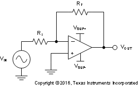
A typical application for an operational amplifier is an inverting amplifier, as shown in Figure 38. An inverting amplifier takes a positive voltage on the input and outputs a signal inverted to the input, making a negative voltage of the same magnitude. In the same manner, the amplifier also makes negative input voltages positive on the output. In addition, amplification can be added by selecting the input resistor RI and the feedback resistor RF.
 Figure 38. Application Schematic
9.2.1 Design Requirements
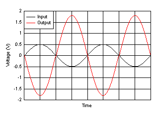
The supply voltage must be chosen to be larger than the input voltage range and the desired output range. The limits of the input common-mode range (VCM) and the output voltage swing to the rails (VO) must also be considered. For instance, this application scales a signal of ±0.5 V (1 V) to ±1.8 V (3.6 V). Setting the supply at ±2.5 V is sufficient to accommodate this application.
9.2.2 Detailed Design Procedure
Determine the gain required by the inverting amplifier using Equation 1 and Equation 2:


When the desired gain is determined, choose a value for RI or RF. Choosing a value in the kΩ range is desirable for general-purpose applications because the amplifier circuit uses currents in the milliamp range. This milliamp current range ensures the device does not draw too much current. The trade-off is that very large resistors (100s of kΩ) draw the smallest current but generate the highest noise. Very small resistors (100s of Ω) generate low noise but draw high current. This example uses 10 kΩ for RI, meaning 36 kΩ is used for RF. These values are determined by Equation 3:

9.2.3 Application Curve
 Figure 39. Inverting Amplifier Input and Output