SLOS270F March 2001 – August 2016 TLV2370 , TLV2371 , TLV2372 , TLV2373 , TLV2374 , TLV2375
PRODUCTION DATA.
- 1 Features
- 2 Applications
- 3 Description
- 4 Revision History
- 5 Device Comparison Tables
- 6 Pin Configuration and Functions
-
7 Specifications
- 7.1 Absolute Maximum Ratings
- 7.2 Recommended Operating Conditions
- 7.3 Thermal Information: TLV2370
- 7.4 Thermal Information: TLV2371
- 7.5 Thermal Information: TLV2372
- 7.6 Thermal Information: TLV2373
- 7.7 Thermal Information: TLV2374
- 7.8 Thermal Information: TLV2375
- 7.9 Electrical Characteristics
- 7.10 Typical Characteristics
- 8 Detailed Description
- 9 Application and Implementation
- 10Power Supply Recommendations
- 11Layout
- 12Device and Documentation Support
- 13Mechanical, Packaging, and Orderable Information
Package Options
Mechanical Data (Package|Pins)
Thermal pad, mechanical data (Package|Pins)
Orderable Information
8 Detailed Description
8.1 Overview
The TLV237x single-supply CMOS operational amplifiers provide rail-to-rail input and output capability with
3-MHz bandwidth. Consuming only 550 μA the TLV237x is the perfect choice for portable and battery-operated applications. The maximum recommended supply voltage is 16 V, which allows the devices to be operated from (±8-V supplies down to ±1.35 V) a variety of rechargeable cells. The rail-to-rail inputs with high input impedance make the TLV237x ideal for sensor signal-conditioning applications.
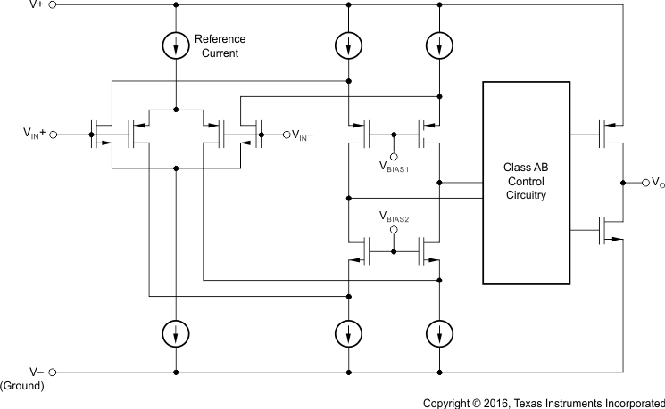
8.2 Functional Block Diagram
8.3 Feature Description
8.3.1 Rail-to-Rail Input Operation
The TLV237x input stage consists of two differential transistor pairs, NMOS and PMOS, that operate together to achieve rail-to-rail input operation. The transition point between these two pairs can be seen in Figure 2, Figure 3, and Figure 4 for a 2.7-V, 5-V, and 15-V supply. As the common-mode input voltage approaches the positive supply rail, the input pair switches from the PMOS differential pair to the NMOS differential pair. This transition occurs approximately 1.35 V from the positive rail and results in a change in offset voltage due to different device characteristics between the NMOS and PMOS pairs. If the input signal to the device is large enough to swing between both rails, this transition results in a reduction in common-mode rejection ratio (CMRR). If the input signal does not swing between both rails, it is best to bias the signal in the region where only one input pair is active. This is the region inFigure 2 through Figure 4 where the offset voltage varies slightly across the input range and optimal CMRR can be achieved. This has the greatest impact when operating from a 2.7-V supply voltage.
8.3.2 Driving a Capacitive Load
When the amplifier is configured in this manner, capacitive loading directly on the output decreases the device phase margin leading to high frequency ringing or oscillations. Therefore, for capacitive loads of greater than 10 pF, TI recommends that a resistor be placed in series (RNULL) with the output of the amplifier, as shown in Figure 34. A minimum value of 20 Ω should work well for most applications.
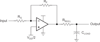 Figure 34. Driving a Capacitive Load
8.3.3 Offset Voltage
The output offset voltage, (VOO) is the sum of the input offset voltage (VIO) and both input bias currents (IIB) times the corresponding gains. Figure 35 can be used to calculate the output offset voltage:
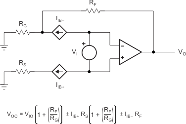 Figure 35. Output Offset Voltage Model
8.3.4 General Configurations
When receiving low-level signals, limiting the bandwidth of the incoming signals into the system is often required. The simplest way to accomplish this is to place an RC filter at the noninverting terminal of the amplifier (see Figure 36).
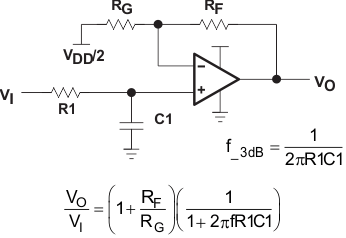 Figure 36. Single-Pole Low-Pass Filter
If even more attenuation is needed, a multiple pole filter is required. The Sallen-Key filter can be used for this task. For best results, the amplifier must have a bandwidth that is 8 to 10 times the filter frequency bandwidth. Failure to do this can result in phase shift of the amplifier.
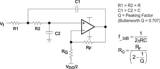 Figure 37. 2-Pole Low-Pass Sallen-Key Filter
8.3.5 Shutdown Function
Three members of the TLV237x family (TLV2370, TLV2373, and TLV2375) have a shutdown terminal for conserving battery life in portable applications. When the shutdown terminal is tied low, the supply current is reduced to 25 μA/channel, the amplifier is disabled, and the outputs are placed in a high impedance mode. To enable the amplifier, the shutdown terminal can either be left floating or pulled high. When the shutdown terminal is left floating, take care to ensure that parasitic leakage current at the shutdown terminal does not inadvertently place the operational amplifier into shutdown.
8.4 Device Functional Modes
The TLV2371, TLV2372, and TLV2374 have a single functional mode. These devices are operational as long as the power-supply voltage is between 2.7 V (±1.35 V) and 16 V (±8 V).
The TLV2370, TLV2373, and TLV2375 are likewise operational as long as the power-supply voltage is between 2.7 V (±1.35 V) and 16 V (±8 V), additionally these devices also have a shutdown capability. When the shutdown control pin is driven below 0.8 V above ground, the device is in shutdown. If the shutdown control pin voltage is driven to greater than 2 V above ground, the device is in its normal operating mode. See Shutdown Function for additional information regarding shutdown operation.