SGLS008G March 2003 – February 2018 TLV2460A-Q1 , TLV2461A-Q1 , TLV2462-Q1 , TLV2462A-Q1 , TLV2463A-Q1 , TLV2464A-Q1
PRODUCTION DATA.
- 1 Features
- 2 Applications
- 3 Description
- 4 Revision History
- 5 Pin Configuration and Functions
-
6 Specifications
- 6.1 Absolute Maximum Ratings
- 6.2 ESD Ratings
- 6.3 Recommended Operating Conditions
- 6.4 Thermal Information: TLV2460x-Q1
- 6.5 Thermal Information: TLV2461x-Q1
- 6.6 Thermal Information: TLV2462-Q1
- 6.7 Thermal Information: TLV2462A-Q1
- 6.8 Thermal Information: TLV2463x-Q1
- 6.9 Electrical Characteristics: VDD = 3 V
- 6.10 Electrical Characteristics: VDD = 5 V
- 6.11 Operating Characteristics: VDD = 3 V
- 6.12 Operating Characteristics: VDD = 5 V
- 6.13 Typical Characteristics
- 7 Parameter Measurement Information
- 8 Detailed Description
- 9 Application and Implementation
- 10Power Supply Recommendations
- 11Layout
- 12Device and Documentation Support
- 13Mechanical, Packaging, and Orderable Information
Package Options
Refer to the PDF data sheet for device specific package drawings
Mechanical Data (Package|Pins)
- D|8
- PW|8
Thermal pad, mechanical data (Package|Pins)
- PW|8
Orderable Information
3 Description
The devices in the TLV246x-Q1 family of low-power rail-to-rail input/output operational amplifiers are designed for battery management systems in HEV/EV and Powertrain, and lighting and roof module systems in body and lighting applications. The input common-mode voltage range extends beyond the supply rails for maximum dynamic range in low-voltage systems. The amplifier output has rail-to-rail performance with high-output-drive capability, solving one of the limitations of older rail-to-rail input/output operational amplifiers. This rail-to-rail dynamic range and high output drive make the TLV246x-Q1 designed for buffering analog-to-digital converters.
The operational amplifier has 6.4-MHz bandwidth and a 1.6-V/μs slew rate with only 500-μA supply current, which provides good ac performance with low-power consumption. Devices are available with an optional shutdown terminal, which places the amplifier in an ultra-low supply-current mode (IDD = 0.3 μA per channel). While in shutdown, the operational amplifier output is placed in a high-impedance state. DC applications are designed with an input noise voltage of 11 nV/√Hz and input offset voltage of 100 μV.
Device Information(1)
| PART NUMBER | PACKAGE | BODY SIZE (NOM) |
|---|---|---|
| TLV246x-Q1, TLV246xA-Q1 | TSSOP (8) | 4.40 mm × 3.00 mm |
| TLV2462-Q1, TLV2462A-Q1 | SOIC (8) | 3.91 mm × 4.90 mm |
| TSSOP (8) | 4.40 mm × 3.00 mm | |
| VSSOP (8) | 3.00 mm × 3.00 mm | |
| TLV246x-Q1, TLV246xA-Q1 | TSSOP (14) | 4.40 mm × 5.00 mm |
- For all available packages, see the orderable addendum at the end of the data sheet.
- For all available device options, see the Mechanical, Packaging, and Orderable Information.
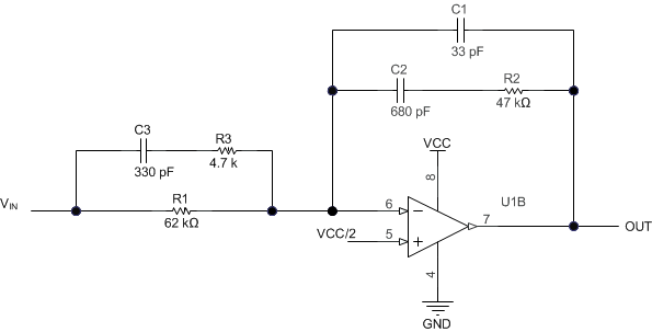
Typical Application
