SLAS355B December 2001 – December 2015 TLV2556
PRODUCTION DATA.
- 1 Features
- 2 Applications
- 3 Description
- 4 Revision History
- 5 Pin Configuration and Functions
-
6 Specifications
- 6.1 Absolute Maximum Ratings
- 6.2 ESD Ratings
- 6.3 Recommended Operating Conditions
- 6.4 Thermal Information
- 6.5 Electrical Characteristics
- 6.6 External Reference Specifications
- 6.7 Internal Reference Specifications
- 6.8 Operating Characteristics
- 6.9 Timing Requirements, VREF+ = 5 V
- 6.10 Timing Requirements, VREF+ = 2.5 V
- 6.11 Typical Characteristics
- 7 Parameter Measurement Information
-
8 Detailed Description
- 8.1 Overview
- 8.2 Functional Block Diagram
- 8.3
Feature Description
- 8.3.1 Converter Operation
- 8.3.2 Power Up and Initialization
- 8.3.3 Default Mode
- 8.3.4 Data Input
- 8.3.5 Data Input - Address/Command Bits
- 8.3.6 Data Output Length
- 8.3.7 LSB Out First
- 8.3.8 Bipolar Output Format
- 8.3.9 Reference
- 8.3.10 INT/EOC Output
- 8.3.11 Chip-Select Input (CS)
- 8.3.12 Power-Down Features
- 8.3.13 Analog MUX
- 8.4 Device Functional Modes
- 9 Application and Implementation
- 10Power Supply Recommendations
- 11Layout
- 12Device and Documentation Support
- 13Mechanical, Packaging, and Orderable Information
Package Options
Refer to the PDF data sheet for device specific package drawings
Mechanical Data (Package|Pins)
- DW|20
- PW|20
Thermal pad, mechanical data (Package|Pins)
Orderable Information
9 Application and Implementation
NOTE
Information in the following applications sections is not part of the TI component specification, and TI does not warrant its accuracy or completeness. TI’s customers are responsible for determining suitability of components for their purposes. Customers should validate and test their design implementation to confirm system functionality.
9.1 Application Information
As with most SAR ADCs, the inputs of the TLV2556 are not high-impedance ports. At the start of the sampling phase, the selected input channel experiences a load current, as the internal analog switches close and the sampling capacitor starts to charge (or discharge). This load current decays over time and varies in a non-linear fashion with respect to input voltage.
The load current is supplied by the input signal source which has non-zero output impedance. As a result, the load current drops non-zero voltage across the output impedance of the signal source creating a time-decaying, non-linear error between the signal source output and the ADC input. This is called sampling error, and if the sampling error does not decay to less than 1 LSB before the end of the sampling window when the sampling switch opens and conversion begins, the ADC output is inaccurate.
The rate of decay of the sampling error and its non-linearity over input voltage are highly sensitive to source impedance. In other words, for larger values of source impedance, the sampling error decays more slowly over time, resulting in greater residual error at the end of the sampling window that is also more non-linear over the ADC input voltage range. Non-linearity in the ADC input translates to non-linearity or harmonic distortion in the ADC output. Harmonic distortion degrades ADC resolution and translates to a decrease in the ADC’s effective number of bits (ENOB). Therefore, driving the ADC input with a low-impedance source is critical for conversion accuracy.
In addition to keeping source impedance as low as possible, TI recommends the following measures for minimizing input sampling error and harmonic distortion associated with the TLV2556 while operating the device at maximum 200-kSPS throughput:
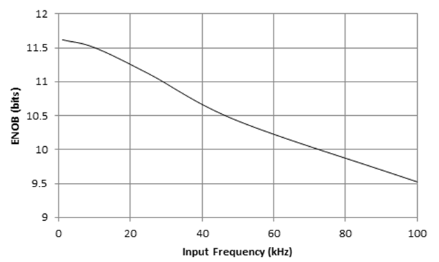
- For AC inputs, the maximum input signal frequency on all channels must be limited to well below the maximum Nyquist rate of 100 kHz. Figure 55 shows how ENOB degrades as input frequency increases.
- For DC inputs, ensure that there are no large step-function changes (greater than VREF / 4) between successive input channels in the scanning order at the highest throughput. If possible, it is advisable to scan the input channels so that the difference in the DC voltage levels between any two successive channels is minimized to ensure 12-bit sampling accuracy. For larger voltage changes between channels, higher accuracy can be achieved by reducing the throughput.
- The stability of the ADC reference input voltage, which is a DC signal, is critical for ADC accuracy. The reference source experiences large instantaneous changes in load current during the ADC conversion phase, and therefore, low source impedance is required for excellent load regulation and stability.

| Rsource = 50 Ω | ƒs = 200KSPS | Ext. 4.096 V Ref. |
9.2 Typical Application
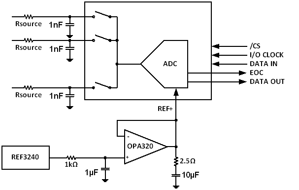
Figure 56 shows a typical application where the TLV2556 is used to acquire multiple AC signals while operating at its maximum sampling rate of 200 kSPS.
 Figure 56. Typical Application Block Diagram
9.2.1 Design Requirements
The design is optimized for superior dynamic performance (low harmonic distortion, high ENOB) while the ADC is multiplexing input channels at maximum sampling rate. Of course, the underlying assumption, based on Application Information, is that the bandwidths of the input signals are much less than 100 kHz. For example, according to Figure 55, the TLV2556 provides better than 11.5 ENOB for AC inputs below 10 kHz.
9.2.2 Detailed Design Procedure
Good dynamic performance while the ADC is multiplexing inputs at maximum sampling rate requires low source impedance on the input channels being addressed. To make the input source impedance less sensitive to line inductance, especially in cases where the signal sources may be located far away from the ADC, it may be necessary to use operational amplifier buffers located close to the ADC input pins.
The procedure for estimating the maximum tolerable value of input source impedance on a given channel for achieving the desired ENOB (for example ENOB > 11.5) in a multiplexed application is as follows:
- Using a low impedance signal source, apply a full-scale sinusoidal signal of suitably low frequency to the ADC input channel of interest, CHx.
- Using a second low impedance source, apply a full-scale sinusoid that has the same frequency as the signal on CHx but is 180˚ out-of-phase, to a second ADC input channel, CHy, that serves as the control element in the experiment.
- Initiate conversions with the ADC continuously multiplexing between CHx and CHy in each conversion cycle.
- Re-arrange the output data by channel, and for each of the two channels, compute SINAD from its FFT and estimate ENOB for that channel as ENOB = (SINAD[dB] – 1.76) / 6.02.
- Increase the series resistance on CHx by a discrete amount and repeat steps 1 through 5 until the ENOB of CHx has degraded sufficiently relative to CHy (which should remain unchanged).
The external 1-nF decoupling capacitors (recommend C0G/NP0 type for constant capacitance versus voltage) on the input channels are required for supplying the instantaneous change in the load current demand of the ADC during the sampling phase after an input channel is selected. In other words, the decoupling capacitor effectively reduces the output impedance of the source at high frequencies.
Similarly, the reference pin also requires decoupling for low output impedance at high frequency. However, the larger magnitude of reference pin load currents during the ADC conversion phase necessitates a decoupling capacitor of a much higher value. The extra ESR (2.5 Ω) is required for stabilizing the OPA320 output as it drives the 10-μF load.
The OPA320 is a wide-band, low-noise, low-power operational amplifier that is unity gain stable and can operate on a single +5-V system supply while supporting rail-to-rail signal swing at its input and output. These properties make it an ideal choice for being used as a high-precision (stable, low-noise) reference buffer that has enough loop gain over frequency to support low output impedance over a wide bandwidth.
9.2.3 Application Curve
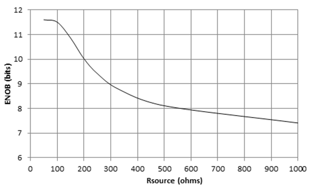
Figure 57 was generated by sweeping Rsource between 50 Ω and 1 kΩ following the procedure detailed in Detailed Design Procedure.

| ƒIN = 1 kHz | ƒs = 200 kSPS | Ext. 4.096 V Ref. |