SLAS355B December 2001 – December 2015 TLV2556
PRODUCTION DATA.
- 1 Features
- 2 Applications
- 3 Description
- 4 Revision History
- 5 Pin Configuration and Functions
-
6 Specifications
- 6.1 Absolute Maximum Ratings
- 6.2 ESD Ratings
- 6.3 Recommended Operating Conditions
- 6.4 Thermal Information
- 6.5 Electrical Characteristics
- 6.6 External Reference Specifications
- 6.7 Internal Reference Specifications
- 6.8 Operating Characteristics
- 6.9 Timing Requirements, VREF+ = 5 V
- 6.10 Timing Requirements, VREF+ = 2.5 V
- 6.11 Typical Characteristics
- 7 Parameter Measurement Information
-
8 Detailed Description
- 8.1 Overview
- 8.2 Functional Block Diagram
- 8.3
Feature Description
- 8.3.1 Converter Operation
- 8.3.2 Power Up and Initialization
- 8.3.3 Default Mode
- 8.3.4 Data Input
- 8.3.5 Data Input - Address/Command Bits
- 8.3.6 Data Output Length
- 8.3.7 LSB Out First
- 8.3.8 Bipolar Output Format
- 8.3.9 Reference
- 8.3.10 INT/EOC Output
- 8.3.11 Chip-Select Input (CS)
- 8.3.12 Power-Down Features
- 8.3.13 Analog MUX
- 8.4 Device Functional Modes
- 9 Application and Implementation
- 10Power Supply Recommendations
- 11Layout
- 12Device and Documentation Support
- 13Mechanical, Packaging, and Orderable Information
Package Options
Refer to the PDF data sheet for device specific package drawings
Mechanical Data (Package|Pins)
- DW|20
- PW|20
Thermal pad, mechanical data (Package|Pins)
Orderable Information
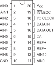
5 Pin Configuration and Functions
DW or PW Package
20-Pin SOIC or TSSOP
Top View

Pin Functions
| PIN | I/O | DESCRIPTION | |
|---|---|---|---|
| NAME | NO. | ||
| AIN0 to AIN10 | 1 to 9, 11, 12 | I | Analog input. These 11 analog-signal inputs are internally multiplexed. |
| CS | 15 | I | Chip select. A high-to-low transition on CS resets the internal counters and controls and enables DATA OUT, DATA IN, and I/O CLOCK. A low-to-high transition disables DATA IN and I/O CLOCK within a setup time. |
| DATA IN | 17 | I | Serial data input. The 4-bit serial data can be used as address selects the desired analog input channel or test voltage to be converted next, or a command to activate other features. The input data is presented with the MSB (D7) first and is shifted in on the first four rising edges of the I/O CLOCK. After the four address/command bits are read into the command register CMR, I/O CLOCK clocks the remaining four bits of configuration in. |
| DATA OUT | 16 | O | 3-state serial output for the A/D conversion result. DATA OUT is in the high-impedance state when CS is high and active when CS is low. With a valid CS, DATA OUT is removed from the high-impedance state and is driven to the logic level corresponding to the MSB/LSB value of the previous conversion result. The next falling edge of I/O CLOCK drives DATA OUT to the logic level corresponding to the next MSB/LSB, and the remaining bits are shifted out in order. |
| GND | 10 | — | Ground. GND is the ground return terminal for the internal circuitry. Unless otherwise noted, all voltage measurements are with respect to GND. |
| INT/EOC | 19 | O | Status output, used to indicate the end of conversion (EOC) or an interrupt (INT) to host processor. Programmed as INT (interrupt): INT goes from a high to a low logic level after the conversion is complete and the data is ready for transfer. INT is cleared by a rising I/O CLOCK transition. Programmed as EOC: EOC goes from a high to a low logic level after the falling edge of the last I/O CLOCK and remains low until the conversion is complete and the data is ready for transfer. |
| I/O CLOCK | 18 | I |
Input /output clock. I/O CLOCK receives the serial input and performs the following four functions:
|
| REF+ | 14 | I/O | Positive reference voltage The upper reference voltage value (nominally VCC) is applied to REF+. The maximum analog input voltage range is determined by the difference between the voltage applied to terminals REF+ and REF–. When the internal reference is used it is capable of driving a 10-kΩ, 10-pF load. |
| REF– | 13 | I/O | Negative reference voltage. The lower reference voltage value (nominally ground) is applied to REF–. This pin is connected to analog ground (GND of the ADC) when internal reference is used. |
| VCC | 20 | — | Positive supply voltage |