SLOS351E February 2004 – November 2016 TLV271 , TLV272 , TLV274
PRODUCTION DATA.
- 1 Features
- 2 Applications
- 3 Description
- 4 Revision History
- 5 Device Comparison Table
- 6 Pin Configuration and Functions
-
7 Specifications
- 7.1 Absolute Maximum Ratings
- 7.2 Recommended Operating Conditions
- 7.3 Thermal Information: TLV271
- 7.4 Thermal Information: TLV272
- 7.5 Thermal Information: TLV274
- 7.6 Electrical Characteristics: DC Characteristics
- 7.7 Electrical Characteristics: Input Characteristics
- 7.8 Electrical Characteristics: Output Characteristics
- 7.9 Electrical Characteristics: Power Supply
- 7.10 Electrical Characteristics: Dynamic Performance
- 7.11 Electrical Characteristics: Noise/Distortion Performance
- 7.12 Typical Characteristics
- 8 Detailed Description
- 9 Application and Implementation
- 10Power Supply Recommendations
- 11Layout
- 12Device and Documentation Support
- 13Mechanical, Packaging, and Orderable Information
Package Options
Refer to the PDF data sheet for device specific package drawings
Mechanical Data (Package|Pins)
- D|8
- P|8
- DBV|5
Thermal pad, mechanical data (Package|Pins)
Orderable Information
11 Layout
11.1 Layout Guidelines
To achieve the levels of high performance of the TLV27x, follow proper printed circuit board (PCB) design techniques. A general set of guidelines is given in the following.
- Ground planes—TI highly recommends using a ground plane on the board to provide all components with a low-inductive ground connection. However, in the areas of the amplifier inputs and output, the ground plane can be removed to minimize the stray capacitance.
- Proper power supply decoupling—Use a 6.8-µF tantalum capacitor in parallel with a 0.1-µF ceramic capacitor on each supply terminal. It may be possible to share the tantalum among several amplifiers depending on the application, but a 0.1-µF ceramic capacitor should always be used on the supply terminal of every amplifier. In addition, the 0.1-µF capacitor should be placed as close as possible to the supply terminal. As this distance increases, the inductance in the connecting trace makes the capacitor less effective. The designer should strive for distances of less than 0.1 inches between the device power terminals and the ceramic capacitors.
- Sockets—Sockets can be used but are not recommended. The additional lead inductance in the socket pins often leads to stability problems. Surface-mount packages soldered directly to the printed-circuit board is the best implementation.
- Short trace runs/compact part placements—Optimum high performance is achieved when stray series inductance has been minimized. To realize this, the circuit layout should be made as compact as possible, thereby minimizing the length of all trace runs. Particular attention should be paid to the inverting input of the amplifier. Its length should be kept as short as possible. This helps to minimize stray capacitance at the input of the amplifier.
- Surface-mount passive components—Using surface-mount passive components is recommended for high performance amplifier circuits for several reasons. First, because of the extremely low lead inductance of surface-mount components, the problem with stray series inductance is greatly reduced. Second, the small size of surface-mount components naturally leads to a more compact layout thereby minimizing both stray inductance and capacitance. If leaded components are used, TI recommends keeping the lead lengths as short as possible.
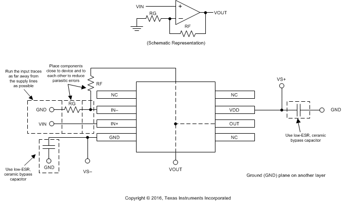
11.2 Layout Example
 Figure 31. TLV27x Layout Example