SLOS922A September 2015 – December 2015 TLV27L2-Q1
PRODUCTION DATA.
- 1 Features
- 2 Applications
- 3 Description
- 4 Revision History
- 5 Selection Guide
- 6 Pin Configuration and Functions
- 7 Specifications
- 8 Detailed Description
- 9 Application and Implementation
- 10Power Supply Recommendations
- 11Layout
- 12Device and Documentation Support
- 13Mechanical, Packaging, and Orderable Information
Package Options
Mechanical Data (Package|Pins)
- D|8
Thermal pad, mechanical data (Package|Pins)
Orderable Information
1 Features
- Qualified for Automotive Applications
- AEC-Q100 Qualified With the Following Results:
- Device Temperature Grade 1: –40°C to +125°C Ambient Operating Temperature Range
- Device HBM Classification Level 2
- Device CDM Classification Level C6
- BiMOS Rail-to-Rail Output
- Input Bias Current: 1 pA
- High Wide Bandwidth 160 kHz
- High Slew Rate: 0.1 V/µs
- Supply Current: 7 µA (per channel)
- Input Noise Voltage: 89 nV/√Hz
- Supply Voltage Range: 2.7 V to 16 V
2 Applications
- Portable Medical
- Power Monitoring
- Low Power Security Detection Systems
- Smoke Detectors
3 Description
The TLV27L2-Q1 single-supply operational amplifiers provide rail-to-rail output capability. The TLV27L2-Q1 device takes the minimum operating supply voltage down to 2.7 V over the extended industrial temperature range, while adding the rail-to-rail output swing feature. The TLV27L2-Q1 device also provides 160-kHz bandwidth from only 7 µA. The maximum recommended supply voltage is 16 V, which allows the devices to be operated from (±8-V supplies down to ±1.35 V) two rechargeable cells.
The rail-to-rail outputs make the TLV27L2-Q1 device good upgrades for the TLC27Lx family of devices which offers more bandwidth at a lower quiescent current. The TLV27L2-Q1 offset voltage is equal to that of the TLC27LxA variant. Their cost effectiveness makes them a good alternative to the TLC225x and TLV225x families of devices, where offset and noise are not of premium importance.
The TLV27L2-Q1 device is available in the commercial temperature range to enable easy migration from the equivalent TLC27Lx.
The TLV27L2-Q1 device is available in an 8-pin SOIC (D) package.
Device Information(1)
| PART NUMBER | PACKAGE | BODY SIZE (NOM) |
|---|---|---|
| TLV27L2-Q1 | SOIC (8) | 4.90 mm × 3.91 mm |
- For all available packages, see the orderable addendum at the end of the datasheet.
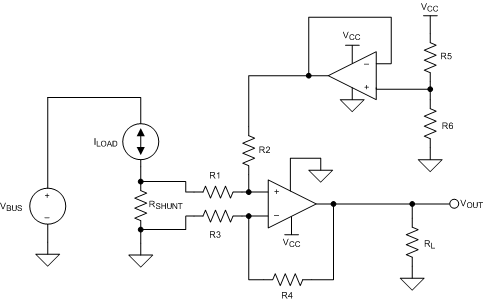
Application Schematic

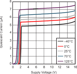
Low and Stable Quiescent Current
