SLAS549D September 2008 – November 2014 TLV320AIC3254
PRODUCTION DATA.
- 1 Features
- 2 Applications
- 3 Description
- 4 Simplified Block Diagram
- 5 Revision History
- 6 Device Comparison Table
- 7 Pin Configuration and Functions
-
8 Specifications
- 8.1 Absolute Maximum Ratings
- 8.2 Handling Ratings
- 8.3 Recommended Operating Conditions
- 8.4 Thermal Information
- 8.5 Electrical Characteristics, ADC
- 8.6 Electrical Characteristics, Bypass Outputs
- 8.7 Electrical Characteristics, Microphone Interface
- 8.8 Electrical Characteristics, Audio DAC Outputs
- 8.9 Electrical Characteristics, LDO
- 8.10 Electrical Characteristics, Misc.
- 8.11 Electrical Characteristics, Logic Levels
- 8.12 I2S LJF and RJF Timing in Master Mode (see )
- 8.13 I2S LJF and RJF Timing in Slave Mode (see )
- 8.14 DSP Timing in Master Mode (see )
- 8.15 DSP Timing in Slave Mode (see )
- 8.16 Digital Microphone PDM Timing (see )
- 8.17 I2C Interface Timing
- 8.18 SPI Interface Timing (See )
- 8.19 Typical Characteristics
- 8.20 Typical Characteristics, FFT
- 9 Parameter Measurement Information
-
10Detailed Description
- 10.1 Overview
- 10.2 Functional Block Diagram
- 10.3 Feature Description
- 10.4 Device Functional Modes
- 10.5 Software
- 10.6 Register Map
- 11Applications and Implementation
- 12Power Supply Recommendations
- 13Layout
- 14Device and Documentation Support
- 15Mechanical, Packaging, and Orderable Information
Package Options
Mechanical Data (Package|Pins)
- RHB|32
Thermal pad, mechanical data (Package|Pins)
- RHB|32
Orderable Information
11 Applications and Implementation
NOTE
Information in the following applications sections is not part of the TI component specification, and TI does not warrant its accuracy or completeness. TI’s customers are responsible for determining suitability of components for their purposes. Customers should validate and test their design implementation to confirm system functionality.
11.1 Application Information
The TLV320AIC3254 is a highly integrated stereo audio codec with integrated miniDSP and flexible digital audio interface options. It enables many different types of audio platforms having a need for stereo audio record and playback and needing to interface with other devices in the system over a digital audio interface.
11.2 Typical Application
Figure 21 shows a typical circuit configuration for a system using theTLV320AIC3254.
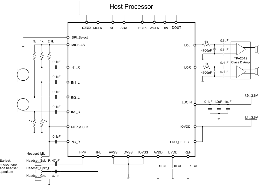 Figure 21. Typical Circuit Configuration
11.2.1 Design Requirements
11.2.1.1 Reference Filtering Capacitor
The TLV320AIC3254 has a built-in bandgap used to generate reference voltages and currents for the device. To achieve high SNR, the reference voltage on REF should be filtered using a 10-μF capacitor from REF terminal to ground.
11.2.1.2 MICBIAS
The TLV320AIC3254 has a built-in bias voltage output for biasing of microphones. No intentional capacitors should be connected directly to the MICBIAS output for filtering.
11.2.2 Detailed Design Procedures
11.2.2.1 Analog Input Connection
The analog inputs to TLV320AIC3254 should be ac-coupled to the device terminals to allow decoupling of signal source's common mode voltage with that of TLV320AIC3254's common mode voltage. The input coupling capacitor in combination with the selected input impedance of TLV320AIC3254 forms a high-pass filter.
For high fidelity audio recording application it is desirable to keep the cutoff frequency of the high pass filter as low as possible. For single-ended input mode, the equivalent input resistance Req can be calculated as
where g is the analog PGA gain calculated in linear terms.
where G is the analog PGA gain programmed in P1_R59-R60 (in dB) and Rin is the value of the resistor programmed in P1_R52-R57 and assumes Rin = Rcm (as defined in P1_R52-R57).
For differential input mode, Req of the half circuit can be calculated as:
where Rin is the value of the resistor programmed in P1_R52-R57, assuming symmetrical inputs.
 Figure 22. Analog Input Connection With Pull-down Resistor
When the analog signal is connected to the system through a connector such as audio jack, it is recommended to put a pull-down resistor on the signal as shown in Figure 22. The pulldown resistor helps keep the signal grounded and helps improve noise immunity when no source is connected to the connector. The pulldown resistor value should be chosen large enough to avoid loading of signal source.
Each analog input of the TLV320AIC3254 is capable of handling signal amplitude of 0.5 Vrms. If the input signal source can drive signals higher than the maximum value, an external resistor divider network as shown in Figure 23 should be used to attenuate the signal to less than 0.5Vrms before connecting the signal to the device. The resistor values of the network should be chosen to provide desired attenuation as well as Equation 6.
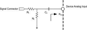 Figure 23. Analog Input Connection With Resistor Divider Network
Whenever any of the analog input terminals IN1_L, IN2_L, IN3_L, IN1_R, IN2_R or IN3_R are not used in an application, it is recommended to short the unused input terminals together (if convenient) and connect them to ground using a small capacitor (example 0.1 µF).
11.2.2.2 Analog Output Connection
The line outputs of the TLV320AIC3254 drive a signal biased around the device common mode voltage. To avoid loading the common mode with the load, it is recommended to connect the single-ended load through an ac-coupling capacitor. The ac-coupling capacitor in combination with the load impedance forms a high pass filter.
For high fidelity playback, the cutoff frequency of the resultant high-pass filter should be kept low. For example with RL of 10 kΩ, using 1-µF coupling capacitor results in a cut-off frequency of 8 Hz.
For differential lineout configurations, the load should be directly connected between the differential outputs, with no coupling capacitor.
Whenever any of the analog output terminals LOL, LOR, HPL or HPR are not used in an application, they should be left open or not connected.
11.2.3 Application Curves
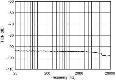
Figure 24 shows the excellent low-distortion performance of the TLV320AIC3254 in a system over the 20-Hz to 20-kHz audio spectrum.
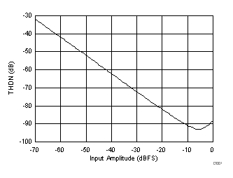
Figure 25 shows the distortion performance of the TLV320AIC3254 in a system over the input amplitude range.
| Differential Lineout | Rload = 10 kΩ | CM = 0.9 V |
| Input Amplitude = -3 dBFS |
Input Frequency
| Differential Lineout | Rload = 10 kΩ | CM = 0.9 V |
| Frequency = 997 Hz |
Input Amplitude