SLAS549D September 2008 – November 2014 TLV320AIC3254
PRODUCTION DATA.
- 1 Features
- 2 Applications
- 3 Description
- 4 Simplified Block Diagram
- 5 Revision History
- 6 Device Comparison Table
- 7 Pin Configuration and Functions
-
8 Specifications
- 8.1 Absolute Maximum Ratings
- 8.2 Handling Ratings
- 8.3 Recommended Operating Conditions
- 8.4 Thermal Information
- 8.5 Electrical Characteristics, ADC
- 8.6 Electrical Characteristics, Bypass Outputs
- 8.7 Electrical Characteristics, Microphone Interface
- 8.8 Electrical Characteristics, Audio DAC Outputs
- 8.9 Electrical Characteristics, LDO
- 8.10 Electrical Characteristics, Misc.
- 8.11 Electrical Characteristics, Logic Levels
- 8.12 I2S LJF and RJF Timing in Master Mode (see )
- 8.13 I2S LJF and RJF Timing in Slave Mode (see )
- 8.14 DSP Timing in Master Mode (see )
- 8.15 DSP Timing in Slave Mode (see )
- 8.16 Digital Microphone PDM Timing (see )
- 8.17 I2C Interface Timing
- 8.18 SPI Interface Timing (See )
- 8.19 Typical Characteristics
- 8.20 Typical Characteristics, FFT
- 9 Parameter Measurement Information
-
10Detailed Description
- 10.1 Overview
- 10.2 Functional Block Diagram
- 10.3 Feature Description
- 10.4 Device Functional Modes
- 10.5 Software
- 10.6 Register Map
- 11Applications and Implementation
- 12Power Supply Recommendations
- 13Layout
- 14Device and Documentation Support
- 15Mechanical, Packaging, and Orderable Information
Package Options
Mechanical Data (Package|Pins)
- RHB|32
Thermal pad, mechanical data (Package|Pins)
- RHB|32
Orderable Information
13 Layout
13.1 Layout Guidelines
Each system design and PCB layout is unique. The layout should be carefully reviewed in the context of a specific PCB design. However, the following guidelines can optimize TLV320AIC3254 performance:
- Connect the thermal pad to ground.
- The decoupling capacitors for the power supplies should be placed close to the device terminals. Figure 21 shows the recommended decoupling capacitors for the TLV320AIC3254.
- The TLV320AIC3254 internal voltage references must be filtered using external capacitors. Place the filter capacitors on REF near the device terminals for optimal performance.
- For analog differential audio signals, the signals should be routed differentially on the PCB for better noise immunity. Avoid crossing of digital and analog signals to avoid undesirable crosstalk.
13.2 Layout Example
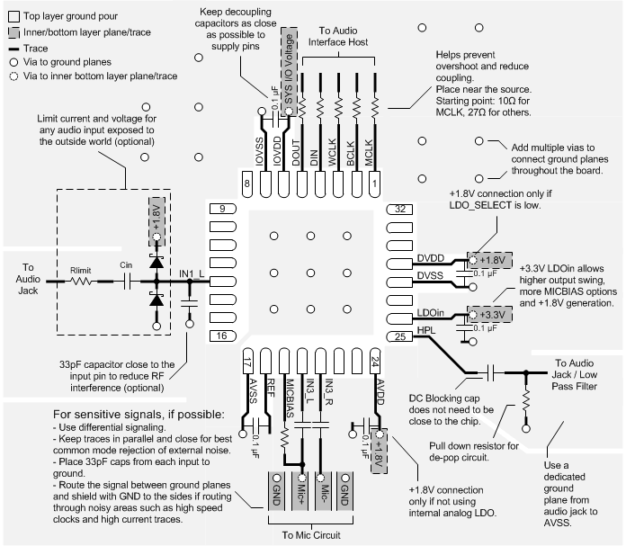 Figure 26. TLV320AIC3254 Layout
Example layout views can be found in the EVM User Guide: