SLAS538B October 2007 – November 2016 TLV320AIC34
PRODUCTION DATA.
- 1 Features
- 2 Applications
- 3 Description
- 4 Revision History
- 5 Description (continued)
- 6 Device Comparison Table
- 7 Pin Configuration and Functions
- 8 Specifications
-
9 Detailed Description
- 9.1 Overview
- 9.2 Functional Block Diagram
- 9.3
Feature Description
- 9.3.1 Hardware Reset
- 9.3.2 I2C Bus Debug In A Glitched System
- 9.3.3 Digital Audio Data Serial Interface
- 9.3.4 TDM Data Transfer
- 9.3.5 Audio Data Converters
- 9.3.6 Audio Clock Generation
- 9.3.7 Stereo Audio ADC
- 9.3.8 Digital Audio Processing For Record Path
- 9.3.9 Automatic Gain Control (AGC)
- 9.3.10 Stereo Audio DAC
- 9.3.11 Digital Audio Processing For Playback
- 9.3.12 Digital Interpolation Filter
- 9.3.13 Delta-Sigma Audio DAC
- 9.3.14 Audio DAC Digital Volume Control
- 9.3.15 Increasing DAC Dynamic Range
- 9.3.16 Analog Output Common-Mode Adjustment
- 9.3.17 Audio DAC Power Control
- 9.3.18 Audio Analog Inputs
- 9.3.19 Analog Input Bypass Path Functionality
- 9.3.20 ADC PGA Signal Bypass Path Functionality
- 9.3.21 Input Impedance and VCM Control
- 9.3.22 Passive Analog Bypass During Power Down
- 9.3.23 MICBIAS_x Generation
- 9.3.24 Digital Microphone Connectivity
- 9.3.25 Analog Fully Differential Line Output Drivers
- 9.3.26 Analog High-Power Output Drivers
- 9.3.27 Short-Circuit Output Protection
- 9.3.28 Jack or Headset Detection
- 9.3.29 Output Stage Volume Controls
- 9.4 Device Functional Modes
- 9.5 Programming
- 9.6 Register Maps
- 10Application and Implementation
- 11Power Supply Recommendations
- 12Layout
- 13Device and Documentation Support
- 14Mechanical, Packaging, and Orderable Information
Package Options
Refer to the PDF data sheet for device specific package drawings
Mechanical Data (Package|Pins)
- ZAS|87
Thermal pad, mechanical data (Package|Pins)
Orderable Information
12 Layout
12.1 Layout Guidelines
PCB design is made considering the application, and the review is specific for each system requirements. However, general considerations can optimize the system performance.
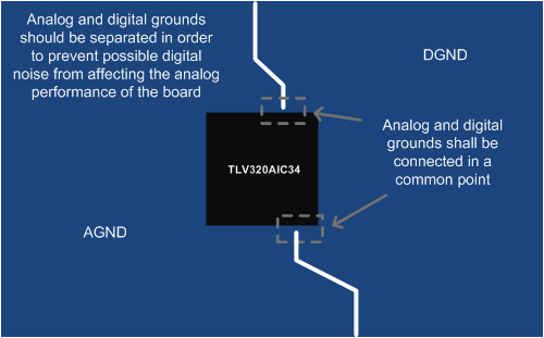
- Analog and digital grounds must be separated to prevent possible digital noise from affecting the analog performance of the board.
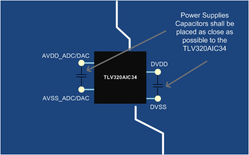
- The TLV320AIC34 requires the decoupling capacitors to be placed as close as possible to the device power supply terminals.
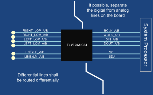
- If possible, route the differential audio signals differentially on the PCB. TI recommends this for better noise immunity.
12.2 Layout Example
 Figure 42. Ground Layer
 Figure 43. Analog Digital Lines
 Figure 44. Power Supplies