SNVSB04C March   2019  – December 2021 TLV4021 , TLV4031 , TLV4041 , TLV4051

PRODUCTION DATA  

  1. Features
  2. Applications
  3. Description
  4. Revision History
  5. Pin Configuration and Functions
  6. Specifications
    1. 6.1 Absolute Maximum Ratings
    2. 6.2 ESD Ratings
    3. 6.3 Recommended Operating Conditions
    4. 6.4 Thermal Information
    5. 6.5 Electrical Characteristics
    6. 6.6 Switching Characteristics
  7. Typical Characteristics
  8. Detailed Description
    1. 8.1 Overview
    2. 8.2 Functional Block Diagram
    3. 8.3 Feature Description
    4. 8.4 Device Functional Modes
      1. 8.4.1 Power ON Reset (POR)
      2. 8.4.2 Input (IN)
      3. 8.4.3 Switching Thresholds and Hysteresis (VHYS)
      4. 8.4.4 Output (OUT)
  9. Application and Implementation
    1. 9.1 Application Information
      1. 9.1.1 Monitoring (V+)
      2. 9.1.2 Monitoring a Voltage Other than (V+)
      3. 9.1.3 VPULLUP to a Voltage Other than (V+)
    2. 9.2 Typical Application
      1. 9.2.1 Under-Voltage Detection
        1. 9.2.1.1 Design Requirements
        2. 9.2.1.2 Detailed Design Procedure
        3. 9.2.1.3 Application Curve
      2. 9.2.2 Additional Application Information
        1. 9.2.2.1 Pull-up Resistor Selection
        2. 9.2.2.2 Input Supply Capacitor
        3. 9.2.2.3 Sense Capacitor
    3. 9.3 What to Do and What Not to Do
  10. 10Power Supply Recommendations
  11. 11Layout
    1. 11.1 Layout Guidelines
    2. 11.2 Layout Example
  12. 12Device and Documentation Support
    1. 12.1 Receiving Notification of Documentation Updates
    2. 12.2 Support Resources
    3. 12.3 Trademarks
    4. 12.4 Electrostatic Discharge Caution
    5. 12.5 Glossary
  13. 13Mechanical, Packaging, and Orderable Information

Package Options

Mechanical Data (Package|Pins)
Thermal pad, mechanical data (Package|Pins)
Orderable Information

Typical Characteristics

at TJ = 25°C and VS = 3.3 V (unless otherwise noted)
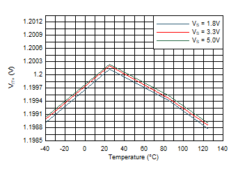
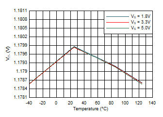
GUID-25F9D615-4B22-4E37-B7AB-971D0686D773-low.gif
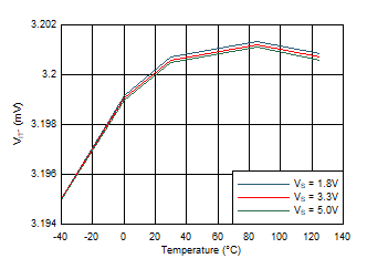
TLV40x1R1
Figure 7-1 Positive Threshold vs Temperature
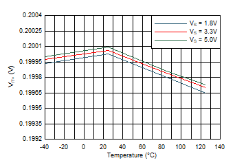
GUID-2F7DCF6D-5A2D-4AFC-BF14-46004A013087-low.gif
TLV40x1R1
Figure 7-3 Negative Threshold vs Temperature
GUID-0FB44C3C-A93A-4523-8081-2473968F29A8-low.gif
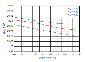
TLV40x1R1
Figure 7-5 Hysteresis vs Temperature
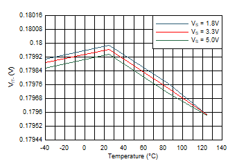
GUID-268A84AF-5F2C-479E-96AA-321BE63267A2-low.gif
TLV40x1R2
Figure 7-7 Positive Threshold vs Temperature
GUID-91377FBB-D895-4147-A3F2-33AAD70AFDF4-low.gif
TLV40x1R2
Figure 7-9 Negative Threshold vs Temperature
GUID-4D13505B-ECEA-442F-BC79-7E91E207D189-low.gif
TLV40x1R2
Figure 7-11 Hysteresis vs Temperature
GUID-FEECB524-1420-44C4-AC0E-DEE58994661B-low.gif
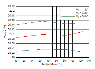
TLV4021S5x
Figure 7-13 Positive Threshold vs Temperature
GUID-691FE712-80EC-4A81-8157-7E504159E89D-low.gif
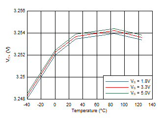
TLV4021S5x
Figure 7-15 Negative Threshold vs Temperature
GUID-B2FA3D2E-C698-4D0A-9082-20B0ECAE5A3C-low.gif
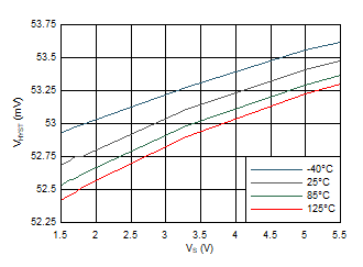
TLV4021S5x
Figure 7-17 Hysteresis vs Supply Voltage
GUID-914793D9-0BE1-44A5-9961-E5B3BAA410D2-low.gif
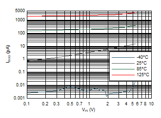
VS = 1.8V to 5VTLV40x1Ry
Figure 7-19 Bias Current vs Common Mode Voltage
GUID-26A1F6A2-95D3-4BF0-AF61-987A7D690B9F-low.gif
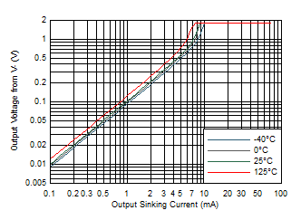
VS = 1.8V
Figure 7-21 Output Voltage vs Output Sinking Current
GUID-88624A18-8846-49AB-AF1B-DD589D670112-low.gif
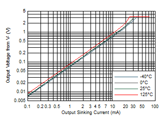
VS = 3.3V
Figure 7-23 Output Voltage vs Output Sinking Current
GUID-6AB2049C-08F1-48D0-8405-6FB1A7C751C7-low.gif
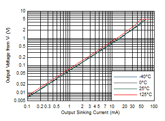
VS = 5V
Figure 7-25 Output Voltage vs Output Sinking Current
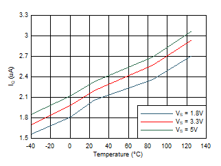
GUID-1655CC15-862E-4F96-BC3C-A516392F1DBD-low.gifFigure 7-27 Supply Current vs Temperature
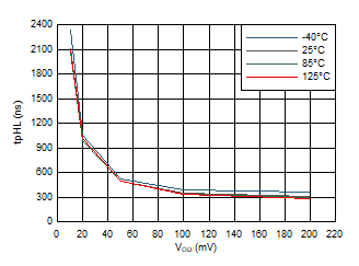
GUID-4D3A46A3-F9F2-4046-B720-A1D501B762E4-low.gif
VS = 1.8V to 5VTLV40x1R2
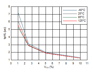
Figure 7-29 Propagation Delay High-Low vs Input Overdrive
GUID-EB51DDC2-BB57-45B6-B73B-9D5F06544DB5-low.gif
VS = 1.8V to 5VTLV4021Sx5
Figure 7-31 Propagation Delay High-Low vs Input Overdrive
GUID-1967A396-B7BE-4D1D-916F-CD2335162D0C-low.gif
TLV40x1R1VS = 5 V
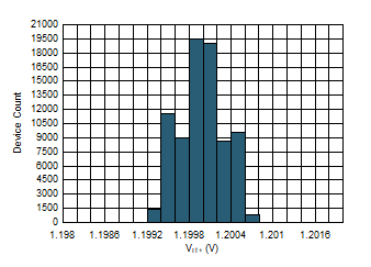
Figure 7-2 Positive Threshold Histogram
GUID-702760DE-F9EE-4641-AF36-3370ECDEC42E-low.gif
TLV40x1R1VS = 5 V
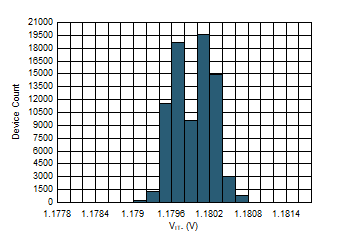
Figure 7-4 Negative Threshold Histogram
GUID-FB5E1437-FD1C-4726-8EDD-C1246F3B0CEA-low.gif
TLV40x1R1VS = 5 V
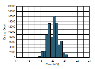
Figure 7-6 Hysteresis Histogram
GUID-A02BD0CF-93CD-45DE-A34B-0F75B1E57BA9-low.gif
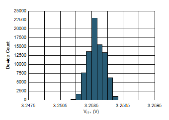
TLV40x1R2VS = 5 V
Figure 7-8 Positive Threshold Histogram
GUID-BE625AEF-5481-468C-B3D0-39B6B9B36A13-low.gif
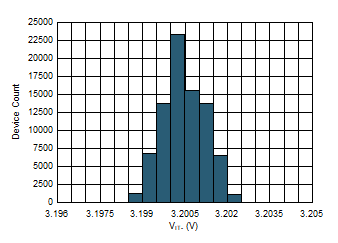
TLV40x1R2VS = 5 V
Figure 7-10 Negative Threshold Histogram
GUID-3EF139D9-7630-4701-A5A0-1A8BB9B676AE-low.gif
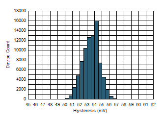
TLV40x1R2VS = 5 V
Figure 7-12 Hysteresis Histogram
GUID-2F4D17AF-4D68-4180-A443-03759B90898A-low.gif
TLV4021S5x
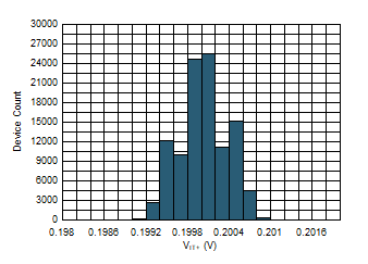
Figure 7-14 Positive Threshold Histogram
GUID-785425E8-19AD-45EE-9046-9FCE35E53D8D-low.gif
TLV4021S5x
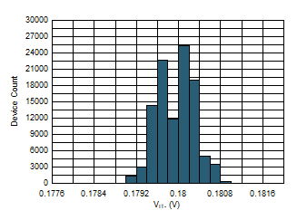
Figure 7-16 Negative Threshold Histogram
GUID-F8FB195A-FF1F-47D0-ADB5-1462DADF6B5A-low.gif
TLV4021S5x
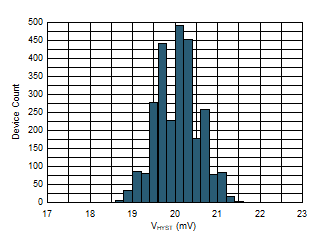
Figure 7-18 Hysteresis Histogram
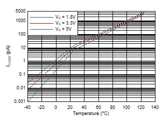
GUID-0EBB72E3-72DA-400A-B23A-451C63E8517A-low.gifFigure 7-20 Output Current Leakage vs Temperature
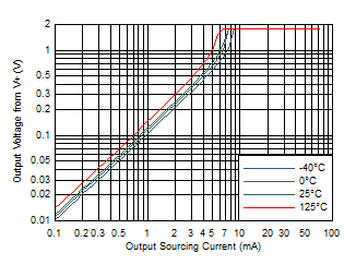
GUID-AF6E0905-3B98-4E4B-AB2F-C7DE1BD38AAC-low.gif
VS = 1.8V
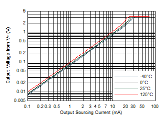
Figure 7-22 Output Voltage vs Output Sourcing Current
GUID-0E06E5AC-0DBB-4C47-8BA5-18928FCBC946-low.gif
VS = 3.3V
Figure 7-24 Output Voltage vs Output Sourcing Current
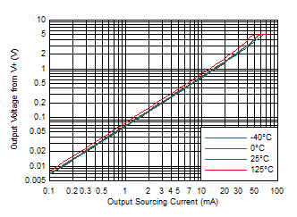
GUID-C5E85302-A232-4462-A3D3-270B92F1DA3D-low.gif
VS = 5V
Figure 7-26 Output Voltage vs Output Sourcing Current
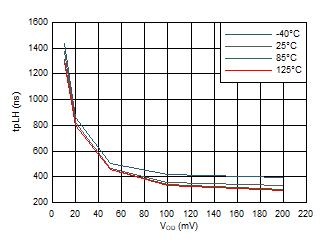
GUID-3DB53F19-0753-4E98-A442-3E009B7EA527-low.gif
VS = 1.8V to 5VTLV40x1R2
Figure 7-28 Propagation Delay Low-High vs Input Overdrive
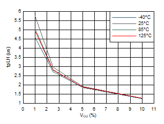
GUID-A900A142-1865-4FCE-974C-73186C900DE5-low.gif
VS = 1.8V to 5VTLV4021Sx5
Figure 7-30 Propagation Delay Low-High vs Input Overdrive