SLVS139Y July 1996 – March 2024 TLV431 , TLV431A , TLV431B
PRODUCTION DATA
- 1
- 1 Features
- 2 Applications
- 3 Description
- 4 Pin Configuration and Functions
- 5 Specifications
- 6 Parameter Measurement Information
- 7 Detailed Description
- 8 Applications and Implementation
- 9 Device and Documentation Support
- 10Revision History
- 11Mechanical, Packaging, and Orderable Information
Package Options
Refer to the PDF data sheet for device specific package drawings
Mechanical Data (Package|Pins)
- DBZ|3
- DBV|5
- PK|3
- DCK|6
- LP|3
Thermal pad, mechanical data (Package|Pins)
Orderable Information
5.8 Typical Characteristics
Operation of the device at these or any other conditions beyond those indicated in the Recommended Operating Conditions table are not implied.
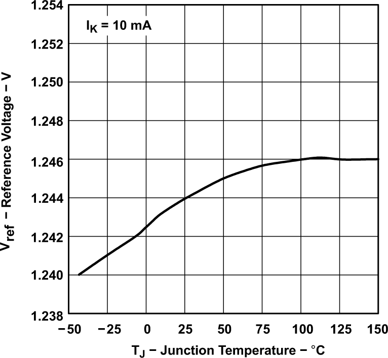 Figure 5-1 Reference Voltage vs Junction Temperature
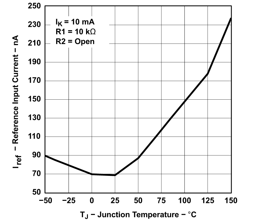 Figure 5-3 Reference Input Current vs Junction Temperature (for TLV431B)
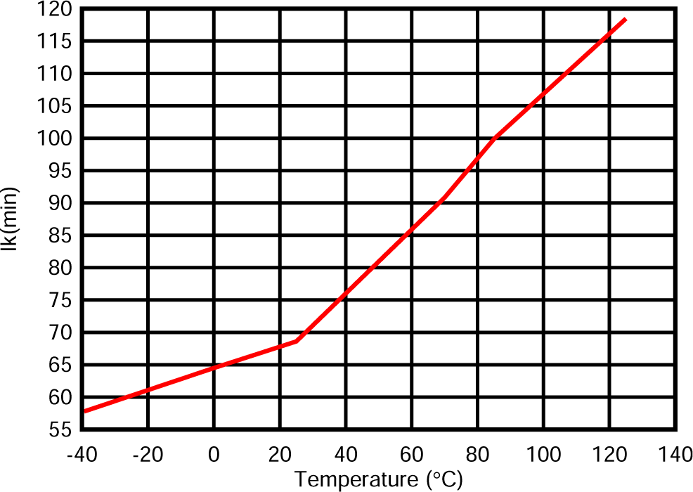 Figure 5-5 Minimum Cathode Current vs Temperature
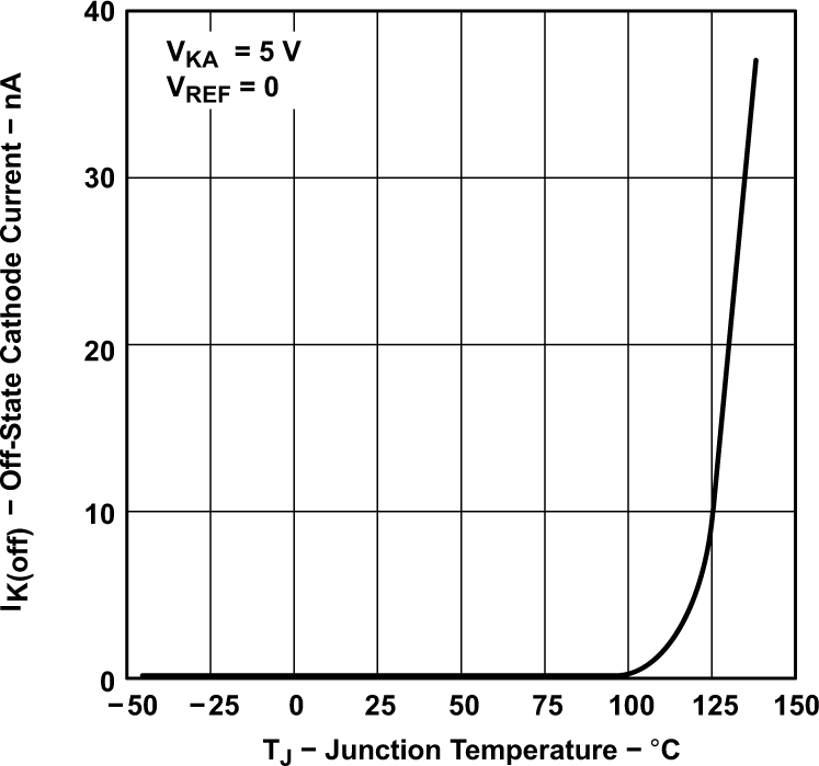 Figure 5-7 Off-State Cathode Current vs Junction Temperature (for TLV431 and
TLV431A)
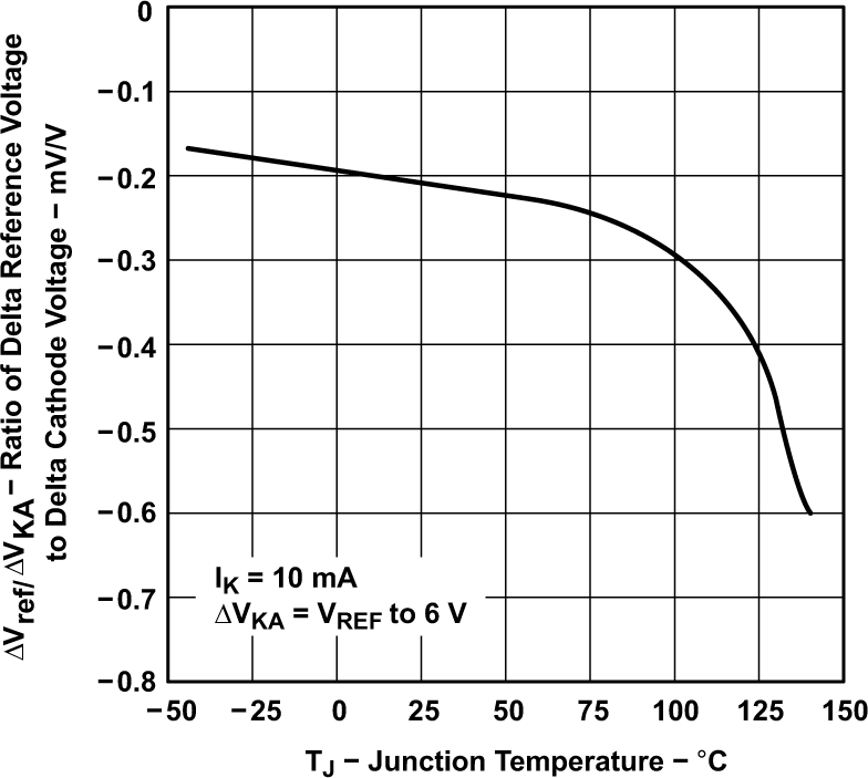 Figure 5-9 Ratio of Delta Reference Voltage to Delta Cathode Voltage vs Junction
Temperature (for TLV431 and TLV431A)
Figure 5-9 Ratio of Delta Reference Voltage to Delta Cathode Voltage vs Junction
Temperature (for TLV431 and TLV431A)‡Extrapolated from Life-test Data Taken at 125°C; the Activation Energy Assumed Is 0.7 eV.
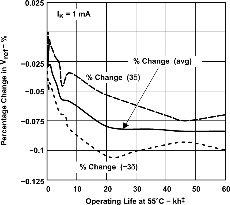 Figure 5-11 Percentage Change in vREF vs Operating Life at 55°C
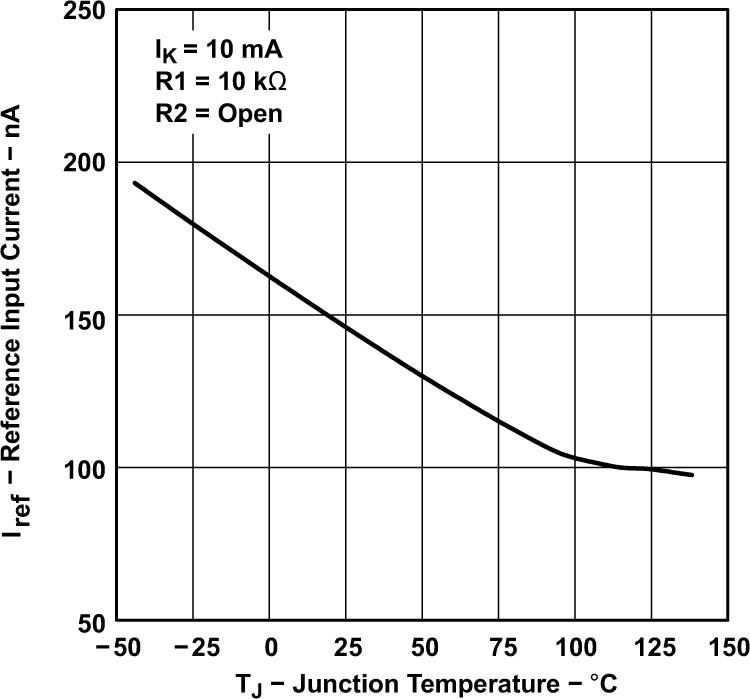 Figure 5-2 Reference Input Current vs Junction Temperature (for TLV431 and
TLV431A)
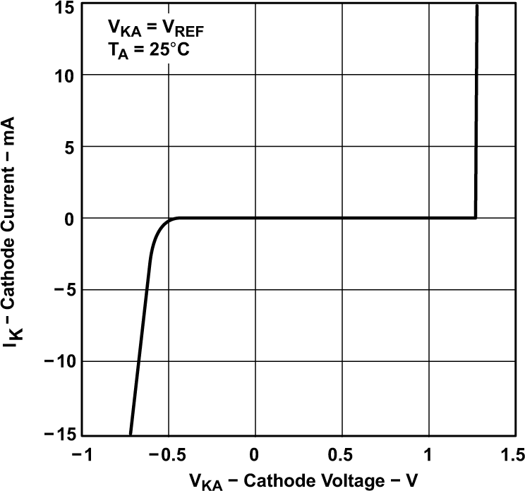 Figure 5-4 Cathode Current vs Cathode Voltage
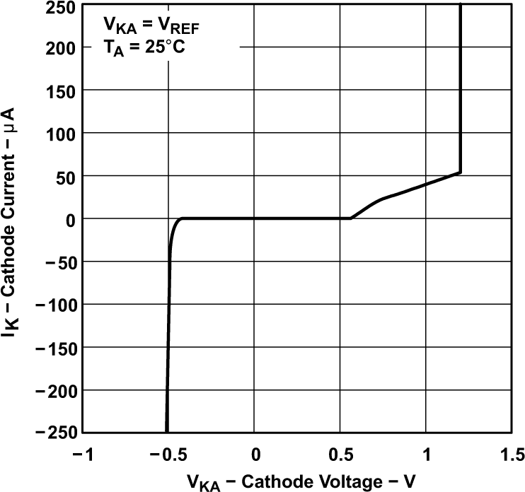 Figure 5-6 Cathode Current vs Cathode Voltage
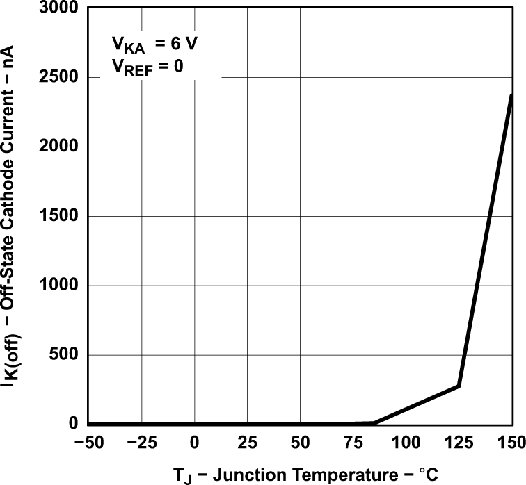 Figure 5-8 Off-State Cathode Current vs Junction Temperature (for TLV431B)
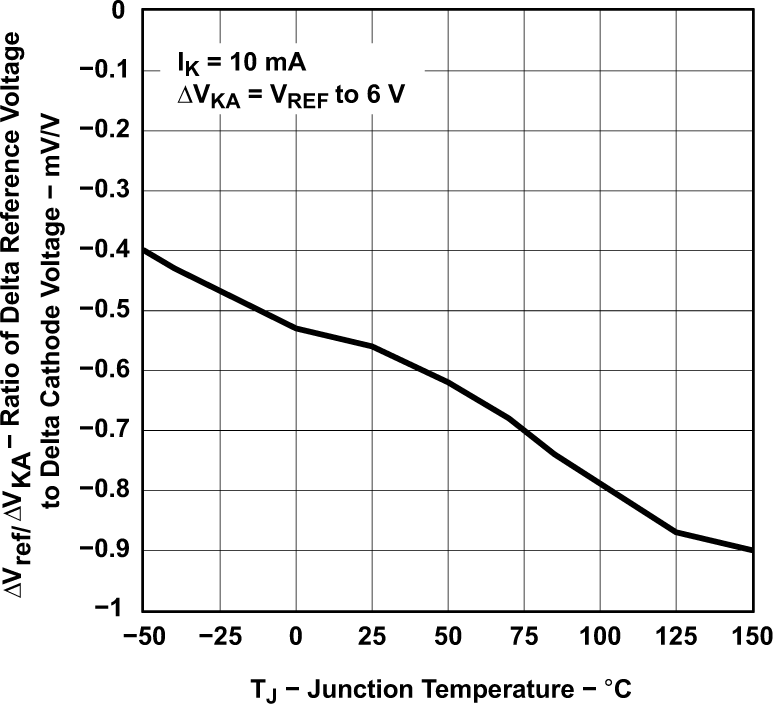 Figure 5-10 Ratio of Delta Reference Voltage to Delta Cathode Voltage vs Junction
Temperature (for TLV431B)
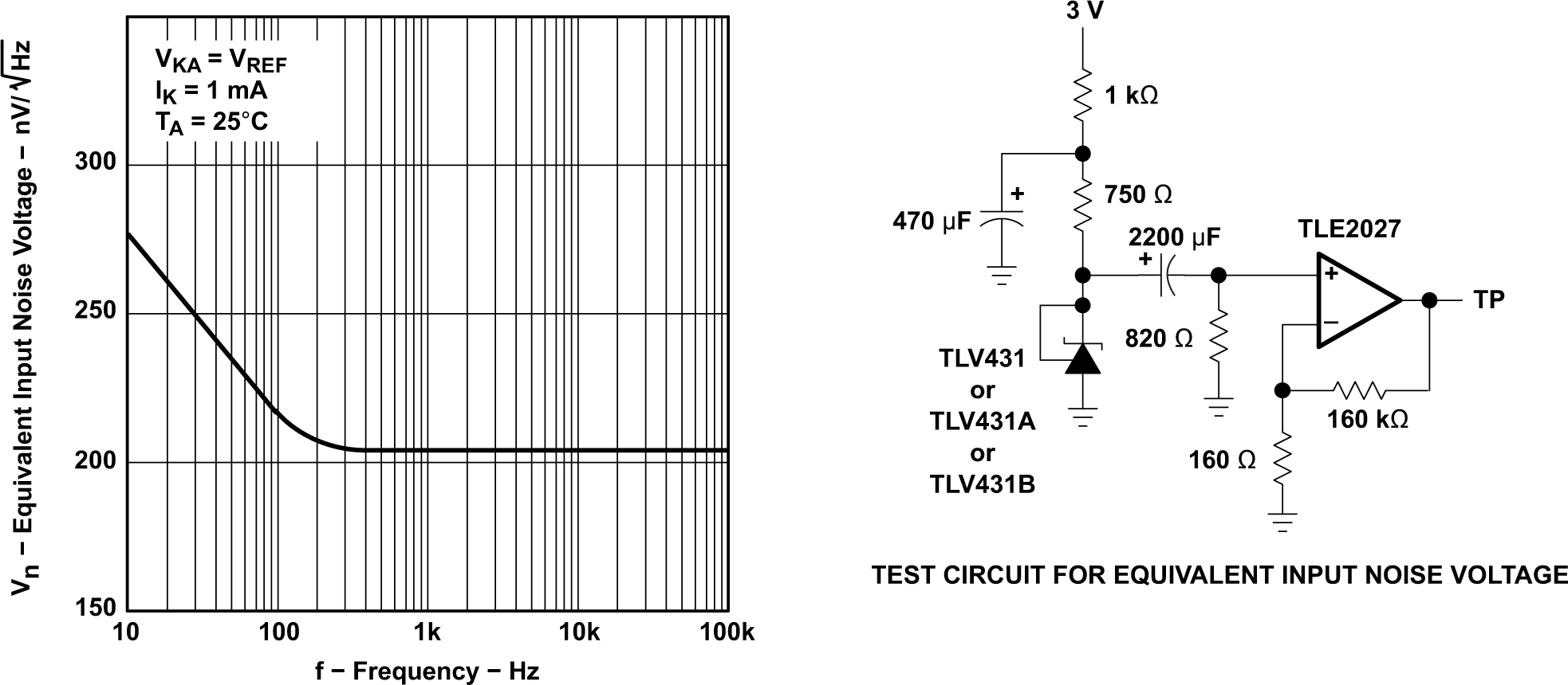 Figure 5-12 Equivalent Input Noise
Voltage
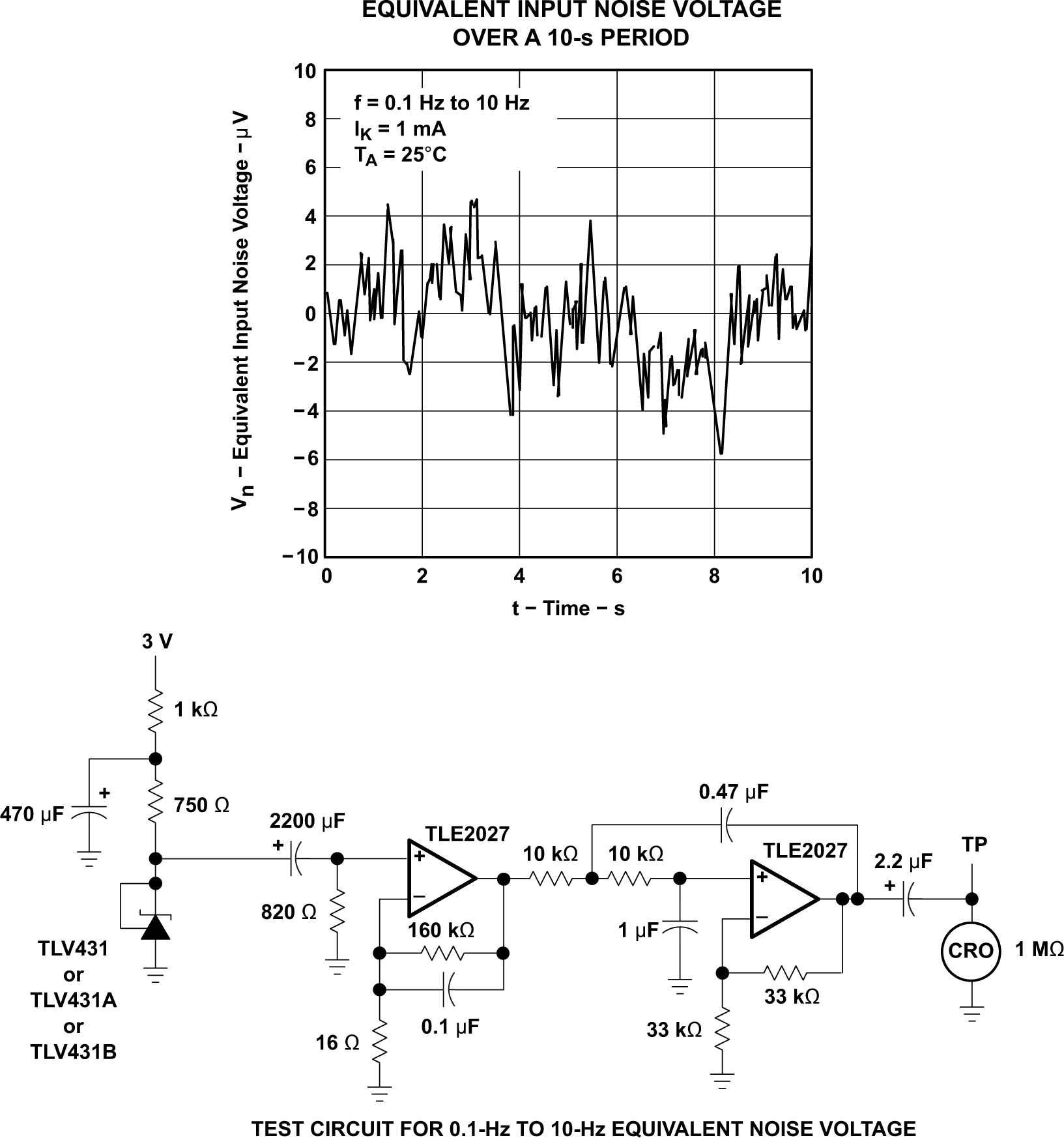 Figure 5-13 Equivalent Noise Voltage
over a 10S Period
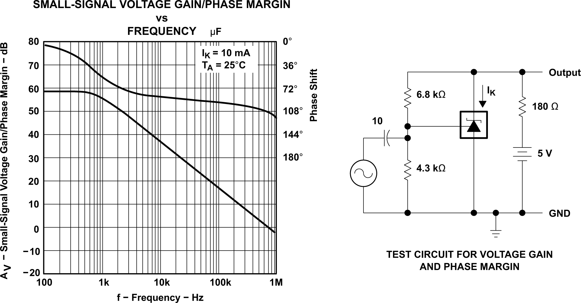 Figure 5-14 Voltage Gain and Phase
Margin
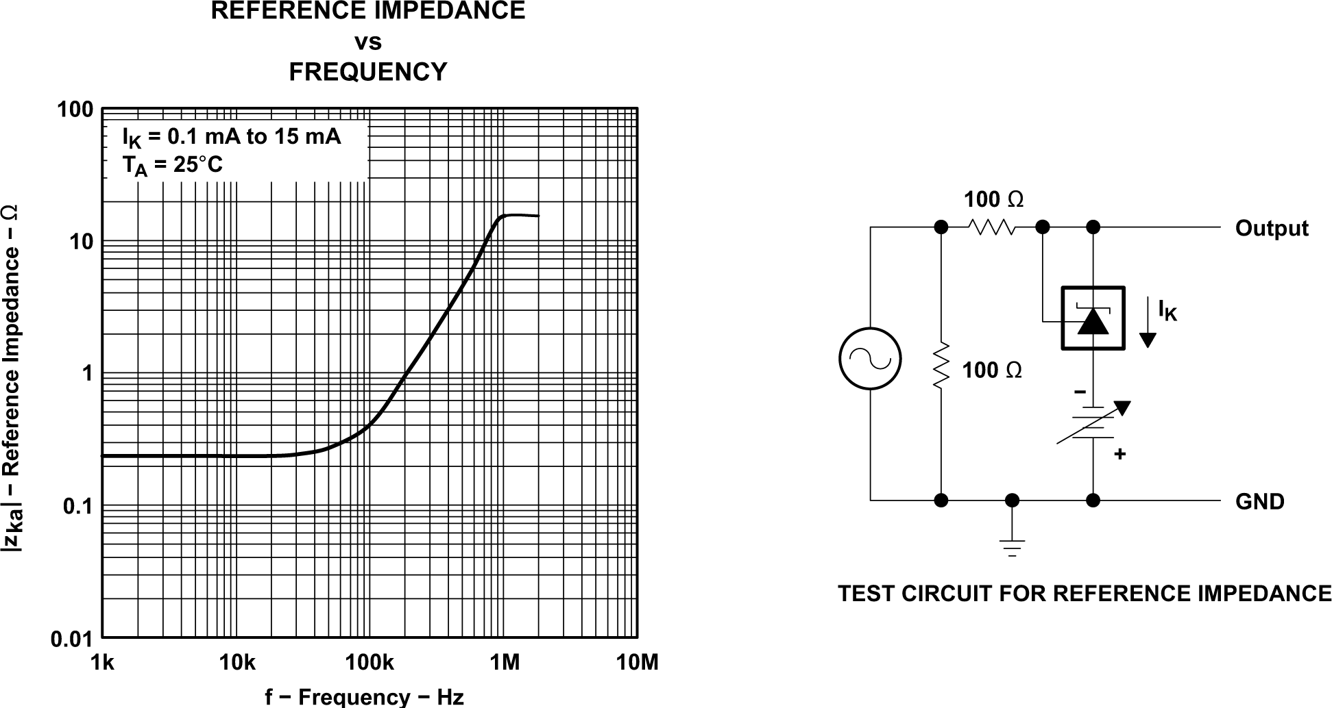 Figure 5-15 Reference Impedance vs
Frequency
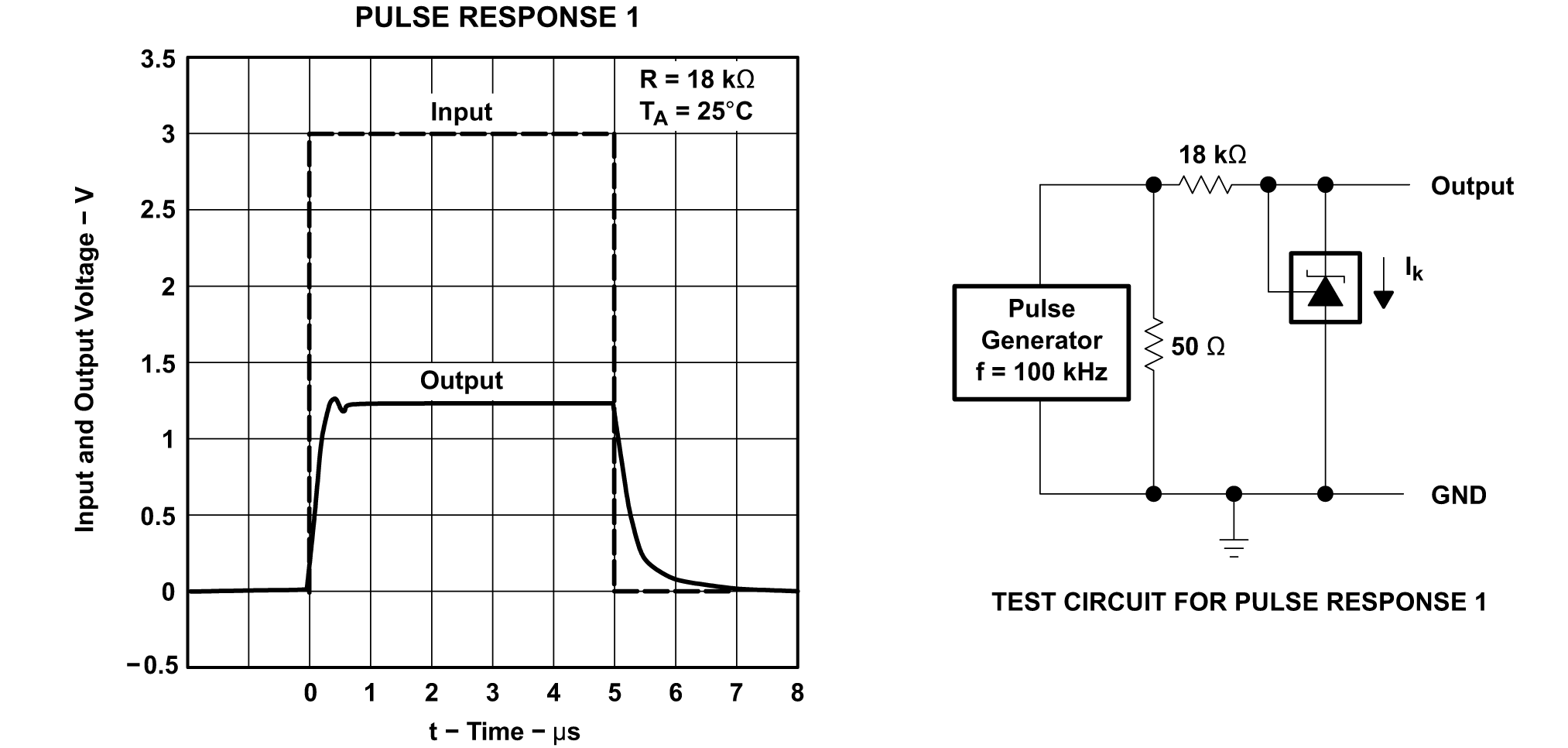 Figure 5-16 Pulse Response 1
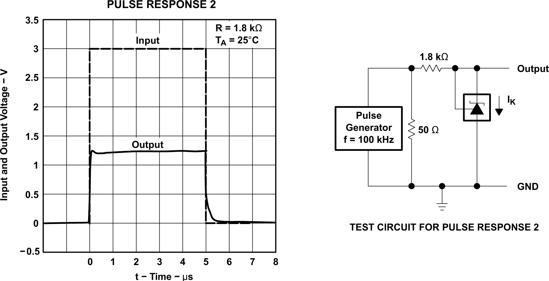 Figure 5-17 Pulse Response 2
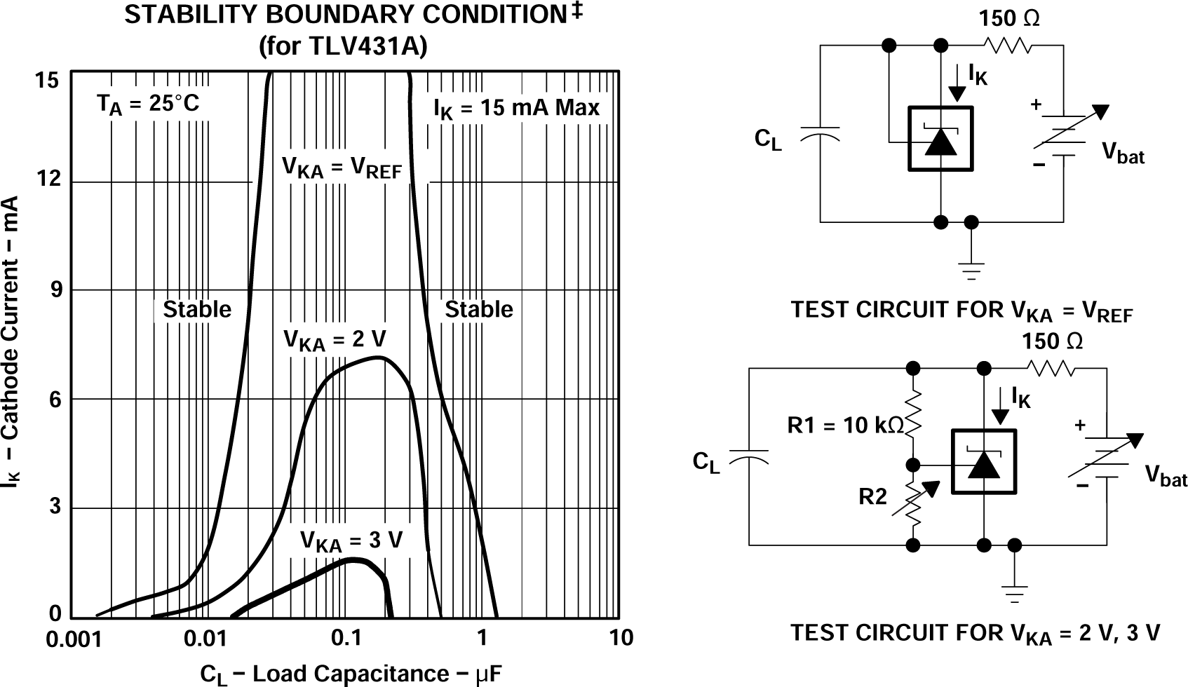
‡The areas under the curves represent conditions that can
cause the device to oscillate. For VKA = 2V and 3V curves, R2 and
Vbat were adjusted to establish the initial VKA
and IK conditions with CL = 0. Vbat and
CL then were adjusted to determine the ranges of
stability.
Figure 5-18 Stability Boundary
Conditions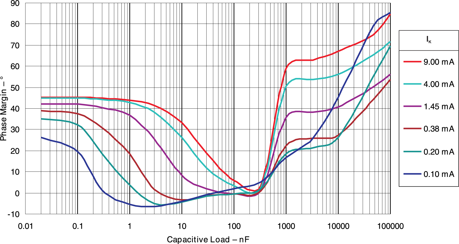 Figure 5-19 Phase Margin vs Capacitive
Load vKA = VREF (1.25V), TA= 25°C
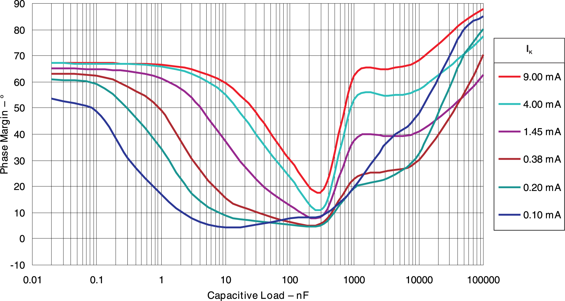 Figure 5-20 Phase Margin vs Capacitive
Load vKA = 2.50V, TA= 25°C
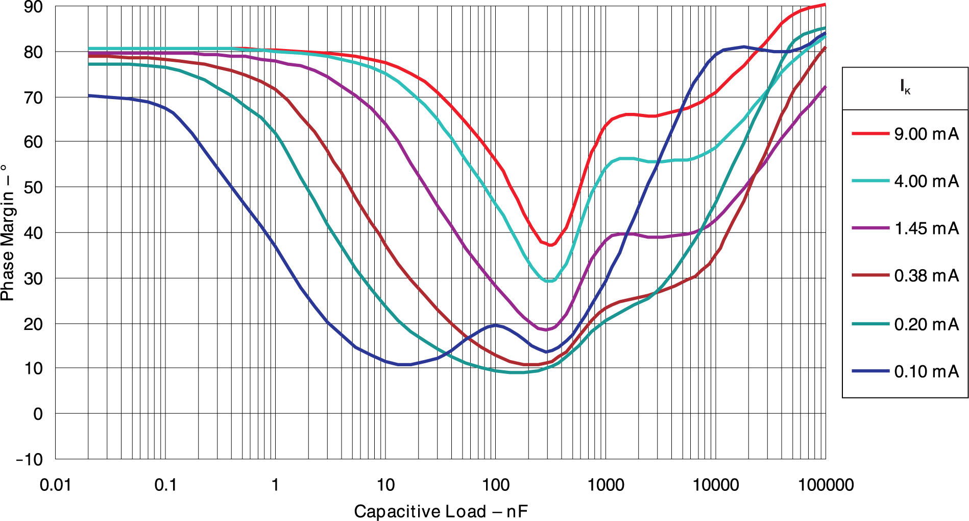 Figure 5-21 Phase Margin vs Capacitive
Load vKA = 5.00V, TA= 25°C