SBOS785B April 2016 – August 2017 TLV2379 , TLV379 , TLV4379
PRODUCTION DATA.
- 1 Features
- 2 Applications
- 3 Description
- 4 Revision History
- 5 Device Comparison Table
- 6 Pin Configuration and Functions
- 7 Specifications
- 8 Detailed Description
- 9 Application and Implementation
- 10Power Supply Recommendations
- 11Layout
- 12Device and Documentation Support
- 13Mechanical, Packaging, and Orderable Information
Package Options
Mechanical Data (Package|Pins)
- PW|14
Thermal pad, mechanical data (Package|Pins)
Orderable Information
8 Detailed Description
8.1 Overview
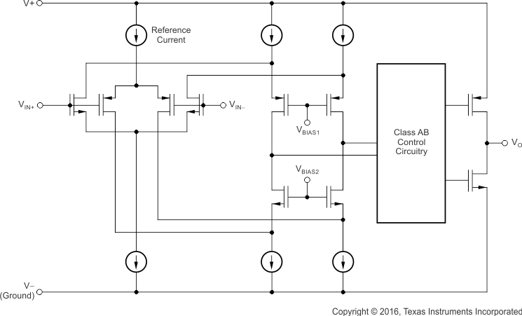
The TLV379 devices are a family of micropower, low-voltage, rail-to-rail input and output operational amplifiers designed for battery-powered applications. This family of amplifiers features impressive bandwidth (90 kHz), low bias current (5 pA), low noise (83 nV/√Hz), and consumes very low quiescent current of only 12 µA (maximum) per channel.
8.2 Functional Block Diagram

8.3 Feature Description
8.3.1 Operating Voltage
The TLV379 series is fully specified and tested from 1.8 V to 5.5 V (±0.9 V to ±2.75 V). Parameters that vary with supply voltage are illustrated in the Typical Characteristics section.
8.3.2 Rail-to-Rail Input
The input common-mode voltage range of the TLV379 family typically extends 100 mV beyond each supply rail. This rail-to-rail input is achieved using a complementary input stage. CMRR is specified from the negative rail to 1 V below the positive rail. Between (V+) – 1 V and (V+) + 0.1 V, the amplifier operates with higher offset voltage because of the transition region of the input stage. See the typical characteristic graph, Offset Voltage vs Common-Mode Voltage vs Temperature (Figure 7).
8.3.3 Rail-to-Rail Output
Designed as a micropower, low-noise operational amplifier, the TLV379 delivers a robust output drive capability. A class AB output stage with common-source transistors is used to achieve full rail-to-rail output swing capability. For resistive loads up to 25 kΩ, the output typically swings to within 5 mV of either supply rail, regardless of the power-supply voltage applied.
8.3.4 Capacitive Load and Stability
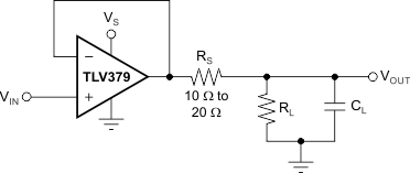
Follower configurations with load capacitance in excess of 30 pF can produce extra overshoot (see the typical characteristic graph, Small-Signal Overshoot vs Capacitive Load, Figure 11) and ringing in the output signal. Increasing the gain enhances the ability of the amplifier to drive greater capacitive loads. In unity-gain configurations, capacitive load drive can be improved by inserting a small (10 Ω to 20 Ω) resistor, RS, in series with the output as shown in Figure 14. This resistor significantly reduces ringing and maintains direct current (dc) performance for purely capacitive loads. However, if a resistive load is in parallel with the capacitive load, a voltage divider is created, introducing a dc error at the output and slightly reducing the output swing. The error introduced is proportional to the ratio of RS / RL and is generally negligible.
 Figure 14. Series Resistor in Unity-Gain Buffer Configuration Improves Capacitive Load Drive
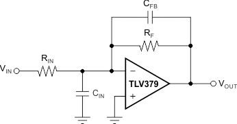
In unity-gain inverter configuration, phase margin can be reduced by the reaction between the capacitance at the operational amplifier (op amp) input and the gain-setting resistors. Best performance is achieved by using smaller-value resistors. However, when large-value resistors cannot be avoided, a small (4 pF to 6 pF) capacitor (CFB) can be inserted in the feedback, as shown in Figure 15. This configuration significantly reduces overshoot by compensating the effect of capacitance (CIN) that includes the amplifier input capacitance (3 pF) and printed circuit board (PCB) parasitic capacitance.
 Figure 15. Improving Stability for Large RF and RIN
8.4 Device Functional Modes
The TLV379 family has a single functional mode. These devices are powered on as long as the power-supply voltage is between 1.8 V (±0.9 V) and 5.5 V (±2.75 V).