SNOSD27 May 2016 TLV522
PRODUCTION DATA.
- 1 Features
- 2 Applications
- 3 Description
- 4 Revision History
- 5 Pin Configuration and Functions
- 6 Specifications
- 7 Detailed Description
- 8 Application and Implementation
- 9 Power Supply Recommendations
- 10Layout
- 11Device and Documentation Support
- 12Mechanical, Packaging, and Orderable Information
Package Options
Mechanical Data (Package|Pins)
- DGK|8
Thermal pad, mechanical data (Package|Pins)
Orderable Information
6 Specifications
6.1 Absolute Maximum Ratings
over operating free-air temperature range (unless otherwise noted)(1)(2)(3)| MIN | MAX | UNIT | ||
|---|---|---|---|---|
| Supply voltage, V+ to V– | -0.3 | 6 | V | |
| Signal input pins | Voltage(2) | V- – 0.3 | V+ + 0.3 | V |
| Current(2) | –10 | 10 | mA | |
| Output short current | Continuous(4) | |||
| Junction temperature | –40 | 150 | °C | |
| Storage temperature, Tstg | –65 | 150 | °C | |
(1) Stresses beyond those listed under Absolute Maximum Ratings may cause permanent damage to the device. These are stress ratings only, which do not imply functional operation of the device at these or any other conditions beyond those indicated under Recommended Operating Conditions. Exposure to absolute-maximum-rated conditions for extended periods may affect device reliability.
(2) Input pins are diode-clamped to the power-supply rails. Input signals that can swing more than 0.3 V beyond the supply rails should be current-limited to 10 mA or less.
(3) If Military/Aerospace specified devices are required, please contact the Texas Instruments Sales Office/Distributors for availability and specifications.
(4) Short-circuit to V–.
6.2 ESD Ratings
| VALUE | UNIT | |||
|---|---|---|---|---|
| V(ESD) | Electrostatic discharge | Human body model (HBM), per ANSI/ESDA/JEDEC JS-001, all pins(1) | ±2000 | V |
| Charged device model (CDM), per JEDEC specification JESD22-C101, all pins(2) |
±250 | |||
(1) JEDEC document JEP155 states that 500-V HBM allows safe manufacturing with a standard ESD control process.
(2) JEDEC document JEP157 states that 250-V CDM allows safe manufacturing with a standard ESD control process.
6.3 Recommended Operating Ratings
over operating free-air temperature range (unless otherwise noted)| MIN | NOM | MAX | UNIT | ||
|---|---|---|---|---|---|
| Supply Voltage ( V+– V− ) | 1.7 | 5.5 | V | ||
| Specified Temperature | –40 | 125 | °C | ||
6.4 Thermal Information
| THERMAL METRIC(1) | TLV522 | UNIT | ||
|---|---|---|---|---|
| DGK (VSSOP) | ||||
| 8 PINS | ||||
| RθJA | Junction-to-ambient thermal resistance | 182.5 | °C/W | |
| RθJC(top) | Junction-to-case (top) thermal resistance | 73.6 | ||
| RθJB | Junction-to-board thermal resistance | 104.1 | ||
| ψJT | Junction-to-top characterization parameter | 13.7 | ||
| ψJB | Junction-to-board characterization parameter | 102.5 | ||
| RθJC(bot) | Junction-to-case (bottom) thermal resistance | N/A | ||
(1) For more information about traditional and new thermal metrics, see the IC Package Thermal Metrics application report, SPRA953.
6.5 Electrical Characteristics
TA = 25°C, V+ = 3.3 V, V− = 0 V, VCM = VO = V+/2, and RL > 1 MΩ , unless otherwise noted.| PARAMETER | TEST CONDITIONS | MIN | TYP(1) | MAX | UNIT | |||
|---|---|---|---|---|---|---|---|---|
| OFFSET VOLTAGE | ||||||||
| Input offset voltage (VOS) | VCM = 0.3 V | –4 | ±1 | 4 | mV | |||
| VCM = 3 V | –4 | ±1 | 4 | |||||
| Drift (dVOS/dT) | 1.5 | µV/°C | ||||||
| Power-Supply Rejection Ratio (PSRR) | V+ = 1.8 V to 3.3 V, VCM = 0.3 V | 80 | 109 | dB | ||||
| INPUT VOLTAGE RANGE | ||||||||
| Common-Mode voltage range (VCM) | CMRR ≥ 62 dB | 0 | 3.3 | V | ||||
| Common-Mode Rejection Ratio (CMRR) | 0 V < VCM < 3.3 V | 62 | 90 | dB | ||||
| 0 V < VCM < 2.2V | 90 | |||||||
| INPUT BIAS CURRENT | ||||||||
| Input bias current (IBIAS) | ±1 | pA | ||||||
| Input offset current (IOS) | ±0.1 | |||||||
| INPUT IMPEDANCE | ||||||||
| Differential | 1013 || 2.5 | Ω || pF | ||||||
| Common mode | 1013 || 2.5 | |||||||
| NOISE | ||||||||
| Input voltage noise density, f = 1 kHz (en) | 300 | nV/√Hz | ||||||
| Current noise density, f = 1 kHz (in) | 65 | fA√Hz | ||||||
| OPEN-LOOP GAIN | ||||||||
| Open-loop voltage gain (AOL) | V+ = 5 V RL = 100 kΩ to V+/2, 0.5 V < VO < 4.5 V |
91 | 101 | dB | ||||
| OUTPUT | ||||||||
| Voltage output swing from positive rail | V+ = 1.8 V, RL = 100 kΩ to V+/2 | 3 | 20 | mV | ||||
| Voltage output swing from negative rail | V+ = 1.8 V, RL = 100 kΩ to V+/2 | 2 | 20 | |||||
| Output current sourcing | Sourcing, V+ = 1.8 V VO to V–, VIN(diff) = 100 mV |
1 | 3 | mA | ||||
| Output current sinking | Sinking, V+ = 1.8 V VO to V+, VIN(diff) = –100 mV |
1 | 5 | |||||
| FREQUENCY RESPONSE | ||||||||
| Gain-bandwidth product (GBWP) | CL = 20 pF | 8 | kHz | |||||
| Slew rate (SR) | G = +1, Rising edge, 1Vp-p, CL = 20 pF | 3.6 | V/ms | |||||
| G = +1, Falling edge, 1Vp-p, CL = 20 pF | 3.7 | |||||||
| POWER SUPPLY | ||||||||
| Quiescent current per channel (IQ) | VCM = 0.3 V, IO = 0 | 500 | 800 | nA | ||||
(1) Refer to Typical Characteristics.
6.6 Typical Characteristics
TA = 25 °C, VOUT = VCM = VS/2, RLOAD = 1 MΩ connected to VS/2, and CL = 20 pF, unless otherwise noted.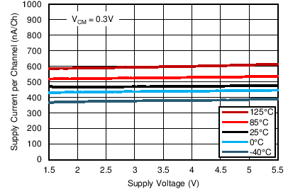
| No Output Load | VCM = 0.3 V |
Low Vcm
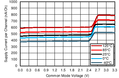
| No Output Load |
Common Mode at 3.3 V
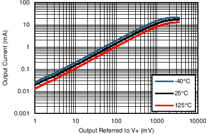
| VS = 3.3 V |
Output Swing at 3.3 V
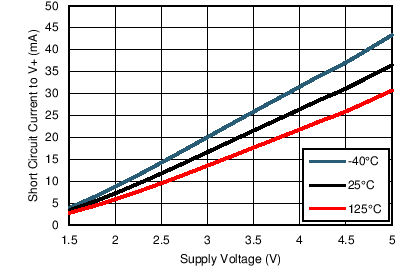
| Ouput set low (sinking), shorted to V+ | ||
Supply Voltage
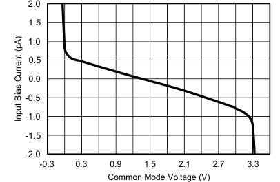
| VS = 3.3 V | TA = 85°C |
Common Mode Voltage at 3.3 V
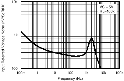
| VS = 5 V | RL = 100 kΩ | CL = 20 pF |
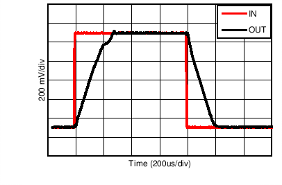
| VS = ±0.9 V | RL = 10 MΩ | CL = 20 pF |
| G = +1 | VIN = ±500mV |
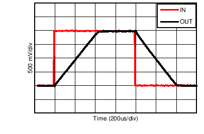
| VS = ±2.5 V | RL = 10 MΩ | CL = 20 pF |
| G = +1 | VIN = ±1V |
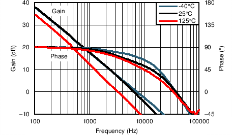
| VS = 5 V | RL = 100 kΩ | CL = 20 pF |
Temperature at 5 V
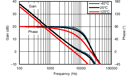
| VS = 5 V | RL = 1 MΩ | CL = 20 pF |
Temperature at 5 V
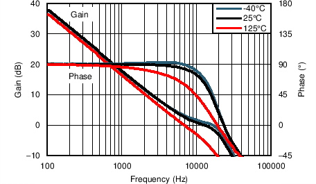
| VS = 5 V | RL = 10 MΩ | CL = 20 pF |
Temperature at 5 V
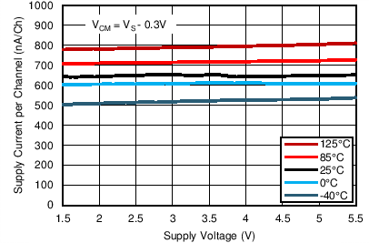
| No Output Load | VCM = (V+) – 0.3 V |
High Vcm
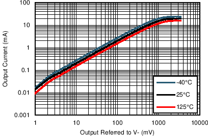
| VS = 3.3 V |
Output Swing at 3.3 V
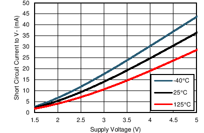
| Output set high (sourcing), shorted to V– | ||
Supply Voltage
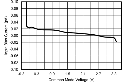
| VS = 3.3 V | TA = 25°C |
Common Mode Voltage at 3.3 V
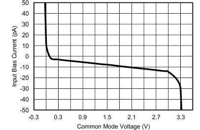
| VS = 3.3 V | TA = 125°C |
Common Mode Voltage at 3.3 V
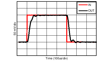
| VS = ±0.9 V | RL = 10 MΩ | CL = 20 pF |
| G = +1 | VIN = ±100 mV |

| VS = ±2.5 V | RL = 10 MΩ | CL = 20 pF |
| G = +1 | VIN = ±100 mV |
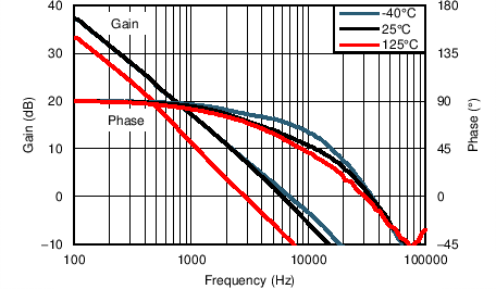
| VS = 1.8 V | RL = 100 kΩ | CL = 20 pF |
Temperature at 1.8 V
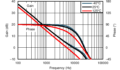
| VS = 1.8 V | RL = 1 MΩ | CL = 20 pF |
Temperature at 1.8 V
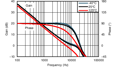
| VS = 1.8 V | RL = 10 MΩ | CL = 20 pF |
Temperature at 1.8 V