SLVSB67D November   2011  – January 2025 TLV70012-Q1 , TLV70018-Q1

PRODUCTION DATA  

  1.   1
  2. Features
  3. Applications
  4. Description
  5. Pin Configuration and Functions
  6. Specifications
    1. 5.1 Absolute Maximum Ratings
    2. 5.2 ESD Ratings
    3. 5.3 Recommended Operating Conditions
    4. 5.4 Thermal Information
    5. 5.5 Electrical Characteristics
    6. 5.6 Typical Characteristics
  7. Detailed Description
    1. 6.1 Overview
    2. 6.2 Functional Block Diagram
    3. 6.3 Feature Description
      1. 6.3.1 Internal Current Limit
      2. 6.3.2 Dropout Voltage
      3. 6.3.3 Undervoltage Lockout (UVLO)
      4. 6.3.4 Thermal Shutdown
    4. 6.4 Device Functional Modes
      1. 6.4.1 Shutdown
      2. 6.4.2 Operation with VIN Less than 2V
      3. 6.4.3 Operation with VIN Greater than 2V
  8. Application and Implementation
    1. 7.1 Application Information
    2. 7.2 Typical Application
      1. 7.2.1 Design Requirements
      2. 7.2.2 Detailed Design Procedure
        1. 7.2.2.1 Input and Output Capacitor Requirements
        2. 7.2.2.2 Transient Response
      3. 7.2.3 Application Curve
    3. 7.3 Power Supply Recommendations
    4. 7.4 Layout
      1. 7.4.1 Layout Guidelines
        1. 7.4.1.1 Thermal Considerations
        2. 7.4.1.2 Power Dissipation
          1. 7.4.1.2.1 Thermal Calculations
      2. 7.4.2 Layout Example
  9. Device and Documentation Support
    1. 8.1 Device Support
      1. 8.1.1 Device Nomenclature
      2. 8.1.2 Package Mounting
    2. 8.2 Documentation Support
      1. 8.2.1 Related Documentation
    3. 8.3 Receiving Notification of Documentation Updates
    4. 8.4 Support Resources
    5. 8.5 Trademarks
    6. 8.6 Electrostatic Discharge Caution
    7. 8.7 Glossary
  10. Revision History
  11. 10Mechanical, Packaging, and Orderable Information

Package Options

Mechanical Data (Package|Pins)
Thermal pad, mechanical data (Package|Pins)
Orderable Information

Typical Characteristics

over operating temperature range (TJ = –40°C to 125°C), VIN = VOUT(NOM) + 0.5V or 2V, whichever is greater; IOUT = 10mA, VEN = VIN, COUT = 1.0μF (unless otherwise noted); typical values are at TJ = 25°C

TLV70018-Q1 TLV70012-Q1 Line
                        Regulation 10mA
 
Figure 5-1 Line Regulation 10mA
TLV70018-Q1 TLV70012-Q1 Load
                        Regulation
 
Figure 5-3 Load Regulation
TLV70018-Q1 TLV70012-Q1 Ground Pin Current vs Input Voltage
 
Figure 5-5 Ground Pin Current vs Input Voltage
TLV70018-Q1 TLV70012-Q1 Ground Pin Current vs Temperature
 
Figure 5-7 Ground Pin Current vs Temperature
TLV70018-Q1 TLV70012-Q1 Current Limit vs Input Voltage
 
Figure 5-9 Current Limit vs Input Voltage
TLV70018-Q1 TLV70012-Q1 Power-Supply Ripple Rejection vs Input Voltage
 
Figure 5-11 Power-Supply Ripple Rejection vs Input Voltage
TLV70018-Q1 TLV70012-Q1 Load
                        Transient Response
 
Figure 5-13 Load Transient Response
TLV70018-Q1 TLV70012-Q1 Load
                        Transient Response
 
Figure 5-15 Load Transient Response
TLV70018-Q1 TLV70012-Q1 Line
                        Transient Response
 
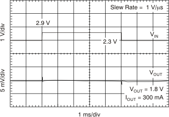
Figure 5-17 Line Transient Response
TLV70018-Q1 TLV70012-Q1 Line
                        Transient Response
 
Figure 5-19 Line Transient Response
TLV70018-Q1 TLV70012-Q1 Line
                        Regulation 300mA
 
Figure 5-2 Line Regulation 300mA
TLV70018-Q1 TLV70012-Q1 Output Voltage vs Temperature
 
Figure 5-4 Output Voltage vs Temperature
TLV70018-Q1 TLV70012-Q1 Ground Pin Current vs Load
 
Figure 5-6 Ground Pin Current vs Load
TLV70018-Q1 TLV70012-Q1 Shutdown Current vs Input Voltage
 
Figure 5-8 Shutdown Current vs Input Voltage
TLV70018-Q1 TLV70012-Q1 Power-Supply Ripple Rejection vs Frequency
 
Figure 5-10 Power-Supply Ripple Rejection vs Frequency
TLV70018-Q1 TLV70012-Q1 Output Spectral Noise Density vs Frequency
 
Figure 5-12 Output Spectral Noise Density vs Frequency
TLV70018-Q1 TLV70012-Q1 Load
                        Transient Response
 
Figure 5-14 Load Transient Response
TLV70018-Q1 TLV70012-Q1 Load
                        Transient Response
 
Figure 5-16 Load Transient Response
TLV70018-Q1 TLV70012-Q1 Line
                        Transient Response
 
Figure 5-18 Line Transient Response
TLV70018-Q1 TLV70012-Q1 VIN Ramp-Up, Ramp-Down Response
 
Figure 5-20 VIN Ramp-Up, Ramp-Down Response