SBVS157E April   2011  – December 2020 TLV803 , TLV853

PRODUCTION DATA  

  1. Features
  2. Applications
  3. Description
  4. Revision History
  5. Device Comparison
  6. Pin Configuration and Functions
    1.     Pin Functions
  7. Specifications
    1. 7.1 Absolute Maximum Ratings (1)
    2. 7.2 ESD Ratings
    3. 7.3 Thermal Information
    4. 7.4 Recommended Operating Conditions
    5. 7.5 Electrical Characteristics
    6. 7.6 Switching Characteristics
    7. 7.7 Typical Characteristics
  8. Detailed Description
    1. 8.1 Overview
    2. 8.2 Functional Block Diagram
    3. 8.3 Feature Description
      1. 8.3.1 VDD Transient Rejection
      2. 8.3.2 Reset During Power Up and Power Down
      3. 8.3.3 Bidirectional Reset Pins
    4. 8.4 Device Functional Modes
      1. 8.4.1 Normal Operation (VDD > Power-Up Reset Voltage)
      2. 8.4.2 Power On Reset (VDD < Power-Up Reset Voltage)
  9. Application and Implementation
    1. 9.1 Application Information
      1. 9.1.1 Monitoring Multiple Supplies
      2. 9.1.2 Output Level Shifting
    2. 9.2 Typical Application
      1. 9.2.1 Design Requirements
      2. 9.2.2 Detailed Design Procedure
      3. 9.2.3 Application Curves
  10. 10Power Supply Recommendations
  11. 11Layout
    1. 11.1 Layout Guidelines
    2. 11.2 Layout Example
  12. 12Device and Documentation Support
    1. 12.1 Device Support
      1. 12.1.1 Development Support
        1. 12.1.1.1 Evaluation Modules
        2. 12.1.1.2 Spice Models
    2. 12.2 Documentation Support
      1. 12.2.1 Related Documentation
    3. 12.3 Related Links
    4. 12.4 Support Resources
    5. 12.5 Trademarks
    6. 12.6 Electrostatic Discharge Caution
    7. 12.7 Glossary
  13. 13Mechanical, Packaging, and Orderable Information

Package Options

Mechanical Data (Package|Pins)
Thermal pad, mechanical data (Package|Pins)
Orderable Information

Output Level Shifting

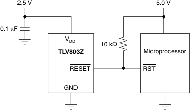
The RESET output of the TLV803 can be pulled to a maximum voltage of 6 V and can be pulled higher in voltage than VDD. It is useful to provide level shifting of the output for cases where the monitored voltage is less than the useful logic levels of the load. Figure 9-2 shows the TLV803Z used to monitor a 2.5-V power rail, with a logic RESET input to a microprocessor that is connected to 5.0 V and has 5.0-V logic levels.
GUID-071199B7-BEBB-4AE7-B100-0E1DD913E198-low.gifFigure 9-2 Output Voltage Level Shifting