SLVSFT6B May 2021 – January 2022 TLVM13630
PRODUCTION DATA
- 1 Features
- 2 Applications
- 3 Description
- 4 Revision History
- 5 Pin Configuration and Functions
-
6 Specifications
- 6.1 Absolute Maximum Ratings
- 6.2 ESD Ratings
- 6.3 Recommended Operating Conditions
- 6.4 Thermal Information
- 6.5 Electrical Characteristics
- 6.6 System Characteristics
- 6.7 Typical Characteristics
- 6.8 Typical Characteristics: VIN = 12 V
- 6.9 Typical Characteristics: VIN = 24 V
- 6.10 Typical Characteristics: VIN = 36 V
-
7 Detailed Description
- 7.1 Overview
- 7.2 Functional Block Diagram
- 7.3
Feature Description
- 7.3.1 Input Voltage Range
- 7.3.2 Adjustable Output Voltage (FB)
- 7.3.3 Input Capacitors
- 7.3.4 Output Capacitors
- 7.3.5 Switching Frequency (RT)
- 7.3.6 Output ON/OFF Enable (EN) and VIN UVLO
- 7.3.7 Power Good Monitor (PG)
- 7.3.8 Internal LDO, VCC Output, and VLDOIN Input
- 7.3.9 Overcurrent Protection (OCP)
- 7.3.10 Thermal Shutdown
- 7.4 Device Functional Modes
-
8 Applications and Implementation
- 8.1 Application Information
- 8.2
Typical Applications
- 8.2.1 Design 1: 3-A Synchronous Buck Regulator for Industrial Applications
- 8.2.2 Design 2: Inverting Buck-Boost Regulator with a –5-V Output
- 9 Power Supply Recommendations
- 10Layout
- 11Device and Documentation Support
- 12Mechanical, Packaging, and Orderable Information
Package Options
Mechanical Data (Package|Pins)
- RDH|30
Thermal pad, mechanical data (Package|Pins)
Orderable Information
5 Pin Configuration and Functions
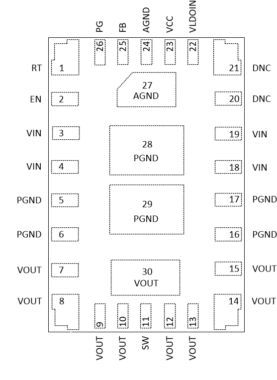
 Figure 5-1 30-Pin QFN,RDH Package(Top View)
Table 5-1 Pin Functions
| PIN | TYPE(1) | DESCRIPTION | |
|---|---|---|---|
| NO. | NAME | ||
| 1 | RT | I | Frequency setting pin. This analog pin is used to set the switching frequency between 200 kHz and 2.2 MHz by placing an external resistor from this pin to AGND. Do not leave open or connect to ground. |
| 2 | EN | I | Precision enable input pin. High = on, low = off. Can be connected to VIN. Precision enable allows the pin to be used as an adjustable UVLO. Place an external voltage divider between this pin, AGND, and VIN to create an external UVLO. |
| 3, 4, 18, 19 | VIN | P | Input supply voltage. Connect the input supply to these pins. Connect input capacitors between these pins and PGND in close proximity to the device. Refer to Section 10.2 for input capacitor placement example. |
| 5, 6, 16, 17, 28, 29 | PGND | G | Power ground. This is the return current path for the power stage of the device. Connect this pad to the input supply return, the load return, and the capacitors associated with the VIN and VOUT pins. See Section 10.2 for a recommended layout. |
| 7-10, 12–15, 30 | VOUT | P | Output voltage. These pins are connected to the internal output inductor. Connect these pins to the output load and connect external output capacitors between these pins and PGND. |
| 11 | SW | O | Switch node. Do not place any external component on this pin or connect to any signal. The amount of copper placed on these pins must be kept to a minimum to prevent issues with noise and EMI. |
| 20,21 | DNC | – | Do Not Connect. Do not connect these pins to ground, to another DNC pin, or to any other voltage. These pins are connected to internal circuitry. Each pin must be soldered to an isolated pad. |
| 22 | VLDOIN | P | Optional LDO supply input. Connect to VOUT or to other voltage rail to improve efficiency. Connect an optional high quality 0.1-μF to 1-μF capacitor from this pin to ground for improved noise immunity. Do not connect to a voltage above 12 V or to a voltage greater than VIN. If unused, connect this pin to ground.. |
| 23 | VCC | O | Internal LDO output. Used as supply to internal control circuits. Do not connect to any external loads. Connect a high-quality 1-μF ceramic capacitor from this pin to PGND. |
| 24, 27 | AGND | G | Analog ground. Zero voltage reference for internal references and logic. All electrical parameters are measured with respect to this pin. This pin must be connected to PGND at a single point. See Section 10.2 for a recommended layout. |
| 25 | FB | I | Feedback input. For the adjustable output version, connect the mid-point of the feedback resistor divider to this pin. Connect the upper resistor (RFBT) of the feedback divider to VOUT at the desired point of regulation. Connect the lower resistor (RFBB) of the feedback divider to AGND. When connecting with feedback resistor divider, keep this FB trace short and as small as possible to avoid noise coupling. See Section 10.2 for a feedback resistor placement. |
| 26 | PG | O | Power-good monitor. Open-drain output that asserts low if the feedback voltage is not within the specified window thresholds. A 10-kΩ to 100-kΩ pullup resistor is required to a suitable pullup voltage. If not used, this pin can be left open or connected to PGND. |
(1) P = Power, G = Ground, I = Input, O = Output