SBASAJ1A December   2022  – February 2023 TMAG5115

PRODUCTION DATA  

  1.   1
  2. Features
  3. Applications
  4. Description
  5. Revision History
  6. Device Comparison
  7. Pin Configuration and Functions
  8. Specifications
    1. 7.1 Absolute Maximum Ratings
    2. 7.2 ESD Ratings
    3. 7.3 Recommended Operating Conditions
    4. 7.4 Thermal Information
    5. 7.5 Electrical Characteristics
    6. 7.6 Magnetic Characteristics
    7. 7.7 Typical Characteristics
  9. Detailed Description
    1. 8.1 Overview
    2. 8.2 Functional Block Diagram
    3. 8.3 Feature Description
      1. 8.3.1 Field Direction Definition
      2. 8.3.2 Device Output
      3. 8.3.3 Power-On Time
      4. 8.3.4 Output Stage
      5. 8.3.5 Protection Circuits
        1. 8.3.5.1 Short-Circuit Protection
        2. 8.3.5.2 Overtemperature Protection
    4. 8.4 Device Functional Modes
  10. Application and Implementation
    1. 9.1 Application Information
    2. 9.2 Typical Applications
      1. 9.2.1 Standard Circuit
        1. 9.2.1.1 Design Requirements
        2. 9.2.1.2 Detailed Design Procedure
          1. 9.2.1.2.1 Configuration Example
        3. 9.2.1.3 Application Curves
    3. 9.3 Power Supply Recommendations
    4. 9.4 Layout
      1. 9.4.1 Layout Guidelines
      2. 9.4.2 Layout Example
  11. 10Device and Documentation Support
    1. 10.1 Device Support
      1. 10.1.1 Hall Sensor Location
    2. 10.2 Receiving Notification of Documentation Updates
    3. 10.3 Support Resources
    4. 10.4 Trademarks
    5. 10.5 Electrostatic Discharge Caution
    6. 10.6 Glossary
  12. 11Mechanical, Packaging, and Orderable Information

Package Options

Mechanical Data (Package|Pins)
Thermal pad, mechanical data (Package|Pins)
Orderable Information
Configuration Example

In a 3.3-V system, 3.0 V ≤ Vref ≤ 3.6 V. Use Equation 2 to calculate the allowable range for R1.

Equation 2. GUID-6519E2CA-B035-4B30-AE6A-78A7957F7D75-low.gif

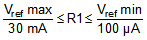
For this design example, use Equation 3 to calculate the allowable range of R1.
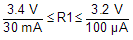
Equation 3. GUID-14A4912D-7C07-41A0-A648-2E76D2845B10-low.gif

Therefore:

Equation 4. 120 Ω ≤ R1 ≤ 30 kΩ

After finding the allowable range of R1 (Equation 4), select a value between 500 Ω and 32 kΩ for R1.

Assuming a system bandwidth of 10 kHz, use Equation 5 to calculate the value of C2.

Equation 5. GUID-4F186788-409F-4609-98E5-8031AF38F444-low.gif

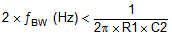
For this design example, use Equation 6 to calculate the value of C2.

Equation 6. GUID-E00B222A-7A5B-4112-A7E1-DB2795B053D4-low.gif

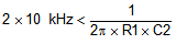
An R1 value of 10 kΩ and a C2 value less than 820 pF satisfy the requirement for a 10-kHz system bandwidth.

A selection of R1 = 10 kΩ and C2 = 680 pF would cause a low-pass filter with a corner frequency of 23.4 kHz.