SLYS042D August 2021 – September 2022 TMAG5231
PRODUCTION DATA
- 1 Features
- 2 Applications
- 3 Description
- 4 Revision History
- 5 Device Comparison
- 6 Pin Configuration and Functions
- 7 Specifications
- 8 Detailed Description
- 9 Application and Implementation
- 10Device and Documentation Support
- 11Mechanical and Packaging Information
Package Options
Mechanical Data (Package|Pins)
Thermal pad, mechanical data (Package|Pins)
- DMR|4
Orderable Information
6 Pin Configuration and Functions
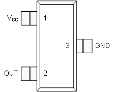
 Figure 6-1 DBZ Package3-Pin SOT-23Top View
Figure 6-2 DMR Package4-Pin X2SONTop View
Table 6-1 Pin Functions
| PIN | I/O | DESCRIPTION | ||
|---|---|---|---|---|
| NAME | SOT-23 (3) | X2SON (4) | ||
| GND | 3 | 1 | — | Ground reference |
| OUT | 2 | 3 | O | Omnipolar output that responds to north and south magnetic poles |
| VCC | 1 | 4 | — | 1.65-V to 5.5-V power supply. TI recommends connecting this pin to a ceramic capacitor to ground with a value of at least 0.1 µF. |
| NC | — | 2 | — | No connect. This pin is not connected to the silicon. It should be left floating or tied to ground. It should be soldered to the board for mechanical support. |
| Thermal Pad | — | PAD | — | No connect. This pin should be left floating or tied to ground. It should be soldered to the board for mechanical support. |