SBOSA72 July   2021 TMCS1108-Q1

PRODUCTION DATA  

  1. Features
  2. Applications
  3. Description
  4. Revision History
  5. Device Comparison
  6. Pin Configuration and Functions
  7. Specifications
    1. 7.1 Absolute Maximum Ratings
    2. 7.2 ESD Ratings
    3. 7.3 Recommended Operating Conditions
    4. 7.4 Thermal Information
    5. 7.5 Power Ratings
    6. 7.6 Electrical Characteristics
    7. 7.7 Typical Characteristics
      1. 7.7.1 Insulation Characteristics Curves
  8. Parameter Measurement Information
    1. 8.1 Accuracy Parameters
      1. 8.1.1 Sensitivity Error
      2. 8.1.2 Offset Error and Offset Error Drift
      3. 8.1.3 Nonlinearity Error
      4. 8.1.4 Power Supply Rejection Ratio
      5. 8.1.5 Common-Mode Rejection Ratio
      6. 8.1.6 External Magnetic Field Errors
    2. 8.2 Transient Response Parameters
      1. 8.2.1 Slew Rate
      2. 8.2.2 Propagation Delay and Response Time
      3. 8.2.3 Current Overload Parameters
      4. 8.2.4 CMTI, Common-Mode Transient Immunity
    3. 8.3 Safe Operating Area
      1. 8.3.1 Continuous DC or Sinusoidal AC Current
      2. 8.3.2 Repetitive Pulsed Current SOA
      3. 8.3.3 Single Event Current Capability
  9. Detailed Description
    1. 9.1 Overview
    2. 9.2 Functional Block Diagram
    3. 9.3 Feature Description
      1. 9.3.1 Current Input
      2. 9.3.2 High-Precision Signal Chain
        1. 9.3.2.1 Lifetime and Environmental Stability
        2. 9.3.2.2 Frequency Response
        3. 9.3.2.3 Transient Response
      3. 9.3.3 Internal Reference Voltage
      4. 9.3.4 Current-Sensing Measurable Ranges
    4. 9.4 Device Functional Modes
      1. 9.4.1 Power-Down Behavior
  10. 10Application and Implementation
    1. 10.1 Application Information
      1. 10.1.1 Total Error Calculation Examples
        1. 10.1.1.1 Room Temperature Error Calculations
        2. 10.1.1.2 Full Temperature Range Error Calculations
    2. 10.2 Typical Application
      1. 10.2.1 Design Requirements
      2. 10.2.2 Detailed Design Procedure
      3. 10.2.3 Application Curve
  11. 11Power Supply Recommendations
  12. 12Layout
    1. 12.1 Layout Guidelines
    2. 12.2 Layout Example
  13. 13Device and Documentation Support
    1. 13.1 Device Support
      1. 13.1.1 Development Support
    2. 13.2 Documentation Support
      1. 13.2.1 Related Documentation
    3. 13.3 Receiving Notification of Documentation Updates
    4. 13.4 Support Resources
    5. 13.5 Trademarks
    6. 13.6 Electrostatic Discharge Caution
    7. 13.7 Glossary
  14. 14Mechanical, Packaging, and Orderable Information

Package Options

Refer to the PDF data sheet for device specific package drawings

Mechanical Data (Package|Pins)
  • D|8
Thermal pad, mechanical data (Package|Pins)
Orderable Information

Nonlinearity Error

Nonlinearity is the deviation of the output voltage from a linear relationship to the input current. Nonlinearity voltage, as shown in Figure 8-1, is the maximum voltage deviation from the best-fit line based on measured parameters, calculated by Equation 7.

Equation 7. VNL = VOUT,MEAS – (IMEAS × Sfit + VOUT,0A)

where

  • VOUT,MEAS is the voltage output at maximum deviation from best fit.
  • IMEAS is the input current at maximum deviation from best fit.
  • Sfit is the best-fit sensitivity of the device.
  • VOUT,0A is the device zero current output voltage.

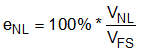
Nonlinearity error (eNL) for the TMCS1108-Q1 is the nonlinearity voltage specified as a percentage of the full-scale output range (VFS), as shown in Equation 8.

Equation 8. GUID-AE7165E5-031D-4D51-BBB9-48F266B67C6C-low.gif