SBOS702E October 2014 – September 2021 TMP102-Q1
PRODUCTION DATA
- 1 Features
- 2 Applications
- 3 Description
- 4 Revision History
- 5 Pin Configuration and Functions
- 6 Specifications
-
7 Detailed Description
- 7.1 Overview
- 7.2 Functional Block Diagram
- 7.3
Feature Description
- 7.3.1 Digital Temperature Output
- 7.3.2 Serial Interface
- 7.3.3 Bus Overview
- 7.3.4 Serial Bus Address
- 7.3.5 Writing and Reading Operation
- 7.3.6 Slave Mode Operations
- 7.3.7 SMBus Alert Function
- 7.3.8 General Call
- 7.3.9 High-Speed (Hs) Mode
- 7.3.10 Time-Out Function
- 7.3.11 Timing Diagrams
- 7.3.12 Two-Wire Timing Diagrams
- 7.4 Device Functional Modes
- 7.5 Programming
- 8 Application and Implementation
- 9 Power Supply Recommendations
- 10Layout
- 11Device and Documentation Support
- 12Mechanical, Packaging, and Orderable Information
Package Options
Mechanical Data (Package|Pins)
- DRL|6
Thermal pad, mechanical data (Package|Pins)
Orderable Information
7.4.1 Continuous-Conversion Mode
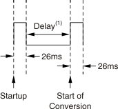
The default mode of the TMP102-Q1 device is continuous conversion mode. During continuous-conversion mode, the ADC performs continuous temperature conversions and stores each results to the temperature register, overwriting the result from the previous conversion. The conversion rate bits, CR1 and CR0, configure the TMP102-Q1 device for conversion rates of 0.25 Hz, 1 Hz, 4 Hz, or 8 Hz. The default rate is 4 Hz. The TMP102-Q1 device has a typical conversion time of 26 ms. To achieve different conversion rates, the TMP102-Q1 device makes a conversion and then powers down to wait for the appropriate delay set by CR1 and CR0. Table 7-5 lists the settings for CR1 and CR0.
| CR1 | CR0 | CONVERSION RATE |
|---|---|---|
| 0 | 0 | 0.25 Hz |
| 0 | 1 | 1 Hz |
| 1 | 0 | 4 Hz (default) |
| 1 | 1 | 8 Hz |
After power-up or general-call reset, the TMP102-Q1 device immediately begins a conversion as shown in Figure 7-6. The first result is available after 26 ms (typical). The active quiescent current during conversion is 40 μA (typical at 27°C). The quiescent current during delay is 2.2 μA (typical at 27°C).
