SBOS545D February 2011 – December 2018 TMP103
PRODUCTION DATA.
- 1 Features
- 2 Applications
- 3 Description
- 4 Revision History
- 5 Pin Configuration and Functions
- 6 Specifications
-
7 Detailed Description
- 7.1 Overview
- 7.2 Functional Block Diagram
- 7.3 Feature Description
- 7.4 Device Functional Modes
- 7.5
Programming
- 7.5.1 Temperature Watchdog Function
- 7.5.2 Conversion Rate
- 7.5.3 Shutdown Mode (M1 = 0, M0 = 0)
- 7.5.4 One-Shot (M1 = 0, M0 = 1)
- 7.5.5 Continuous Conversion Mode (M1 = 1)
- 7.5.6 Bus Overview
- 7.5.7 Serial Interface
- 7.5.8 Serial Bus Address
- 7.5.9 Writing and Reading Operation
- 7.5.10 Slave Mode Operations
- 7.5.11 General Call
- 7.5.12 High-Speed (Hs) Mode
- 7.5.13 Timeout Function
- 7.5.14 Multiple Device Access
- 7.5.15 NOISE
- 7.6 Register Maps
- 8 Application and Implementation
- 9 Power Supply Recommendations
- 10Layout
- 11Device and Documentation Support
- 12Mechanical, Packaging, and Orderable Information
Package Options
Refer to the PDF data sheet for device specific package drawings
Mechanical Data (Package|Pins)
- YFF|4
Thermal pad, mechanical data (Package|Pins)
Orderable Information
7.6.1 Pointer Register
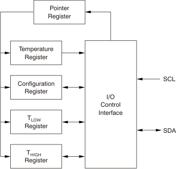
Figure 15 shows the internal register structure of the TMP103. The 8-bit Pointer Register of the device is used to address a given data register. The Pointer Register uses the two LSBs to identify which of the data registers should respond to a read or write command. Table 3 identifies the bits of the Pointer Register byte. During a write command, P2 through P7 must always be 0. Table 4 describes the pointer address of the registers available in the TMP103. Power-up reset value of P1/P0 is 00. By default, the TMP103 reads the temperature on power up.
 Figure 15. Internal Register Structure
 Table 3. Pointer Register Byte
| P7 | P6 | P5 | P4 | P3 | P2 | P1 | P0 |
|---|---|---|---|---|---|---|---|
| 0 | 0 | 0 | 0 | 0 | 0 | Register Bits | |
Table 4. Pointer Addresses
| P1 | P0 | REGISTER |
|---|---|---|
| 0 | 0 | Temperature Register (Read Only) |
| 0 | 1 | Configuration Register (Read/Write) |
| 1 | 0 | TLOW Register (Read/Write) |
| 1 | 1 | THIGH Register (Read/Write) |