SBOS545D February 2011 – December 2018 TMP103
PRODUCTION DATA.
- 1 Features
- 2 Applications
- 3 Description
- 4 Revision History
- 5 Pin Configuration and Functions
- 6 Specifications
-
7 Detailed Description
- 7.1 Overview
- 7.2 Functional Block Diagram
- 7.3 Feature Description
- 7.4 Device Functional Modes
- 7.5
Programming
- 7.5.1 Temperature Watchdog Function
- 7.5.2 Conversion Rate
- 7.5.3 Shutdown Mode (M1 = 0, M0 = 0)
- 7.5.4 One-Shot (M1 = 0, M0 = 1)
- 7.5.5 Continuous Conversion Mode (M1 = 1)
- 7.5.6 Bus Overview
- 7.5.7 Serial Interface
- 7.5.8 Serial Bus Address
- 7.5.9 Writing and Reading Operation
- 7.5.10 Slave Mode Operations
- 7.5.11 General Call
- 7.5.12 High-Speed (Hs) Mode
- 7.5.13 Timeout Function
- 7.5.14 Multiple Device Access
- 7.5.15 NOISE
- 7.6 Register Maps
- 8 Application and Implementation
- 9 Power Supply Recommendations
- 10Layout
- 11Device and Documentation Support
- 12Mechanical, Packaging, and Orderable Information
Package Options
Refer to the PDF data sheet for device specific package drawings
Mechanical Data (Package|Pins)
- YFF|4
Thermal pad, mechanical data (Package|Pins)
Orderable Information
7.5.1 Temperature Watchdog Function
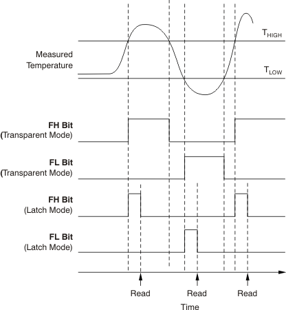
The TMP103 contains a watchdog function that monitors device temperature and compares the result to the values stored in the temperature limit registers (THIGH and TLOW) to determine if the device temperature is within these set limits. If the temperature of the TMP103 becomes greater than the value in the THIGH register, then the flag-high bit (FH) in the configuration register is set to 1. If the temperature falls below the value in the TLOW register, then the flag-low bit (FL) is set to 1. If both flag bits remain 0, then the temperature is within the temperature window set by the temperature limit registers, as shown in Figure 12.
 Figure 12. Temperature Flag Functional Diagram
 The latch bit (LC) in the configuration register is used to latch the value of the flag bits (FH and FL) until the master issues a read command to the configuration register. The flag bits are set to 0 if a read command is received by the TMP103, or if LC = 0 and the temperature is within the temperature limits. The power-on default values for these bits are FH = 0, FL = 0, and LC = 0.