SBOS564B November 2011 – December 2018 TMP104
PRODUCTION DATA.
- 1Features
- 2Applications
- 3Description
- 4Revision History
- 5Pin Configuration and Functions
- 6Specifications
- 7Detailed Description
- 8Device and Documentation Support
- 9Mechanical, Packaging, and Orderable Information
Package Options
Refer to the PDF data sheet for device specific package drawings
Mechanical Data (Package|Pins)
- YFF|4
Thermal pad, mechanical data (Package|Pins)
Orderable Information
7.4.2.2 Conversion Rate (CR1, CR0)
The conversion rate bits (CR1 and CR0), located in the Configuration Register, configure the TMP104 for conversion rates of 8 Hz, 4 Hz, 1 Hz, or 0.25 Hz (default). The TMP104 has a typical conversion time of 26 ms. To achieve different conversion rates, the TMP104 performs a single conversion and then powers down and waits for the appropriate delay set by CR1 and CR0. Table 8 shows the settings for CR1 and CR0.
Table 8. Conversion Rate Settings
| CR1 | CR0 | CONVERSION RATE |
|---|---|---|
| 0 | 0 | 0.25 Hz (default) |
| 0 | 1 | 1 Hz |
| 1 | 0 | 4 Hz |
| 1 | 1 | 8 Hz |
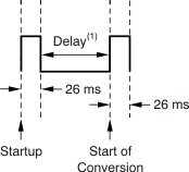
After power-up or general-call reset, the TMP104 immediately starts a conversion, as shown in Figure 14. The first result is available after 26 ms (typical). The active quiescent current during conversion is 40 μA (typical at +25°C, V+ = 1.8 V). The quiescent current during delay is 1.0 μA (typical at +25°C, V+ = 1.8 V).

NOINDENT:
Delay is set by CR1 and CR0.